
Electrical Equipment Circuit
Index 79
VIDEO_CABLE_DRIVER
Published:2009/6/24 21:45:00 Author:Jessie
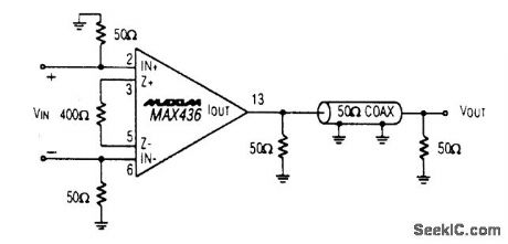
This is a MAX436 coaxial-cable driving circuit (View)
View full Circuit Diagram | Comments | Reading(1421)
VIDEO_IF_AMPLIFIER_DETECTOR
Published:2009/6/24 21:44:00 Author:Jessie
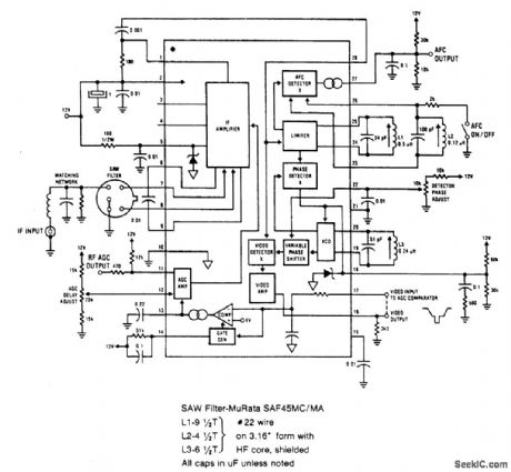
View full Circuit Diagram | Comments | Reading(1175)
NTSC_TO_RGB_CONVERTER
Published:2009/6/24 21:43:00 Author:Jessie
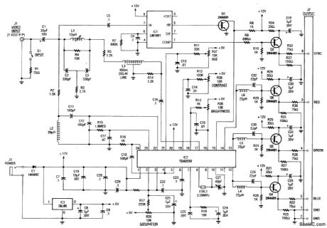
This circuit takes baseband NTSC video, decodes it, and derives RGB video suitable for driving a color multisync computer monitor. This enables the user to take advantage of the generally better resolution of computer monitors. (View)
View full Circuit Diagram | Comments | Reading(5310)
ULTRASONIC_cw_TRANSCEIVER
Published:2009/6/24 21:33:00 Author:Jessie
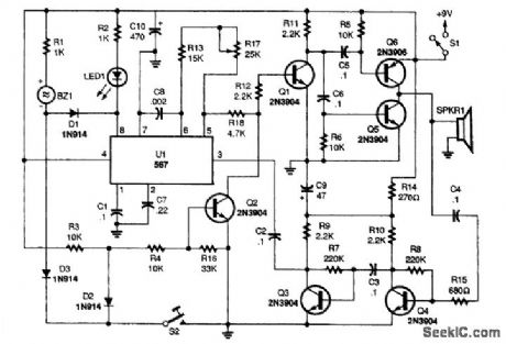
With the telegraph key at S2 up (open), the 567 PLL's input at pin 3 is coupled to the output of Q3. Transistors Q3 and Q4 are operat-ing in a high-gain, two-stage audio-amplifier circuit. The piezo speaker is coupled to the in-put of the amplifier though a 0.1-μF capacitor and a 680-Ω isolation resistor.In the receive mode, the piezo speaker oper-ates as a sensitive microphone. Ultrasonic signals travel from the microphone through the two-stage amplifier to the input of the 567, and, if the signal's frequency is within the IC's bandwidth, the LED will light and piezo-sounder BZ1 will sing out foreach dit and dah received. The receiver can be tuned to the incoming ultrasonic signal by adjust-ing R17. Of course, adjusting that potentiometer also changes the transmitter's frequency.The transmitter operates each time the S2 is closed. When the key is closed, diode D3 supplies a path to ground for BZ1, causing that sounder to produce an audible signal for each dit and dah transmitted. Also, Q2's bias is taken to ground through D2, allowing Q1 to pass the 567's square-wave signal on to the input of the power amplifier and out through the speaker. (View)
View full Circuit Diagram | Comments | Reading(2446)
MICRO_TV_TRANSMITTER
Published:2009/6/24 21:19:00 Author:May
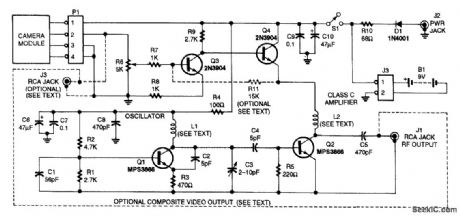
For very low power noncritical applications, this small TV modulator can be useful as a shortrange (50 feet) transmitter for video signals. A small camera module can be used as a source. R11 is used to vary dc offset of the modulator. (View)
View full Circuit Diagram | Comments | Reading(0)
VISUAL_ZERO_BEAT_INDICATOR
Published:2009/6/24 21:27:00 Author:Jessie
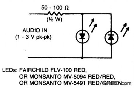
Light-emitting diodes connected with re-verse polarity provide a visual indication of zero-beat ffequency. Each LED is on for only half a cycle of the input. When the input fre-quency is more than 1 kilohertz away from the zero-beat frequency, both LEDs appear to be on all the time. As the input frequency comes within about 20 hertz of zero beat, the LEDs will flicker until zero beat is reached. Both LEDs glow or flicker until zero beat is reached, when they go out. (View)
View full Circuit Diagram | Comments | Reading(0)
ZERO_CENTER_INDICATOR_FOR_FM_RECEIVERS
Published:2009/6/24 21:26:00 Author:Jessie
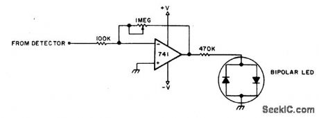
To adjust, tune in a station and adjust the 1 M pot for a null. Then ask the station to modulate and fine adjust so modulation peaks don't light the LEDs. Stations are properly tuned when neither LED is lit. (View)
View full Circuit Diagram | Comments | Reading(1361)
LOW_COST_6_W,40_M_CW_TRANSMITTER
Published:2009/6/24 21:26:00 Author:Jessie

L1 and L2 are wound on a 7/8 diameter form. L1 is 15 turns #22 plastic-covered wire, and L2 is 7 turns #22 plastic-covered wire. (View)
View full Circuit Diagram | Comments | Reading(1839)
WIRELESS_MICROPHONE
Published:2009/6/24 21:20:00 Author:Jessie
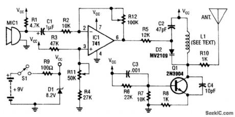
An op-amp IC (741) amplifies the audio signal from MIC1, and R12 controls its gain. Audio is fed to the oscillator circuit Q1 and related components. D2 is a varactor diode. Audio fed to D2 causes FM of the oscillator signal. L1 is 1/2 turns of #18 wire on a He diameter form. The antenna is a 12 whip. (View)
View full Circuit Diagram | Comments | Reading(3)
MICRO_TV_TRANSMITTER
Published:2009/6/24 21:19:00 Author:Jessie
For very low power noncritical applications, this small TV modulator can be useful as a shortrange (50 feet) transmitter for video signals. A small camera module can be used as a source. R11 is used to vary dc offset of the modulator. (View)
View full Circuit Diagram | Comments | Reading(2751)
WIRELESS_GUITAR_TRANSMITTER
Published:2009/6/24 21:16:00 Author:Jessie
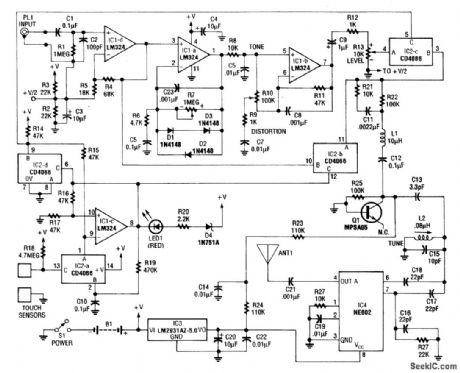
This transmitter has a built-in distortion effects unit and a touch switch to switch effects off and on. The circuit operates from a 9-V battery. IC1-a and IC1-b are used in the effects circuitry. IC1-d is an input preamp and IC2 is a quad analog switch to handle audio switching. Q1 acts as a varactor diode modulator while IC-4 is an 88- to 108-MHz FM oscillator. (View)
View full Circuit Diagram | Comments | Reading(2974)
CABLE_TRACER
Published:2009/6/24 21:12:00 Author:Jessie
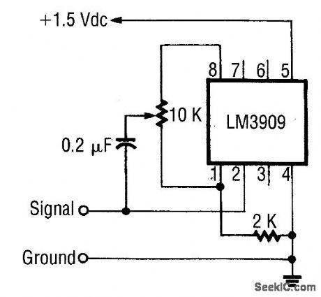
This circuit generates a 1-kHz square wave for cable tracing. Because this circuit is simple and generates from 1.5 V, several can be used at the same time to generate multiple tones for tracing multiconductor cables. (View)
View full Circuit Diagram | Comments | Reading(2707)
WIRE_TRACER
Published:2009/6/24 21:12:00 Author:Jessie

This tracer works by placing a square-wave signal on the line to be traced. The square wave is rich in harmonics. A small transistor radio placed close to a wire carrying this signal will buzz. The ra-dio, therefore, is used as a probe to trace out the wire. (View)
View full Circuit Diagram | Comments | Reading(1)
OVERTONE_CRYSTAL_OSCILLATOR
Published:2009/6/24 20:49:00 Author:Jessie
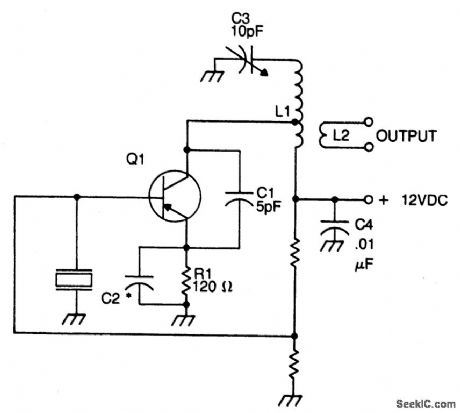
The crystal element in this circuit is con-nected directly between the base and ground.Capacitor C1 is used to improve the feedback due to the internal capacitances of the transis-tor. This capacitor should be mounted as close as possible to the case of the transistor. The LC tank circuit in the collector of the transistor is tuned to the overtone frequency of the crystal.The emitter resistor capacitor must have a capacitive reactance of approximately 90 ohms at the frequency of operation. The tap on induc-tor L1 is used to match the impedance of the collector of the transistor. In most cases, the optimum placement of this tap is approximately one-third from the cold end of the coil. The placement of this tap is a trade-off between stability and maximum power output. The out-put signal is taken from a link coupling coil, L2, and operates by transformer action. (View)
View full Circuit Diagram | Comments | Reading(2193)
HIGH_FREQUENCY_CRYSTAL_OSCILLATOR
Published:2009/6/24 20:42:00 Author:Jessie
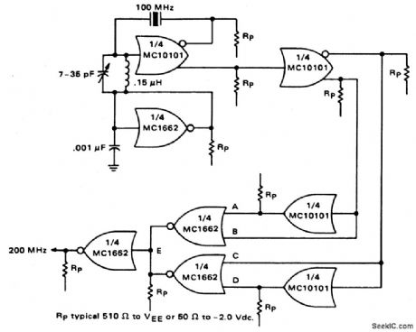
Circuit NotesOne section of the MC10101 is connected as a 100 MHz crystal oscillator with the crystal in series with the feedback loop. The LO tank circuit tunes the 100 MHz harmonic of the crystal and may be used to calibrate the circuit to the exact frequency. A second section of the MC10101 buffers the crystal oscillator and gives complementary 100 MHz signals. Thefrequency doubler consists of two MC10101 gates as phase shifters and two MC1662 NOR gates. For a 50% duty cycle at the output, the delay to the true and complement 100 MHz signals should be 90'. This may be built pre-cisely with 2.5 ns delay lines for the 200 MHz output or approximated by the two MC10101 gates as shown. (View)
View full Circuit Diagram | Comments | Reading(1758)
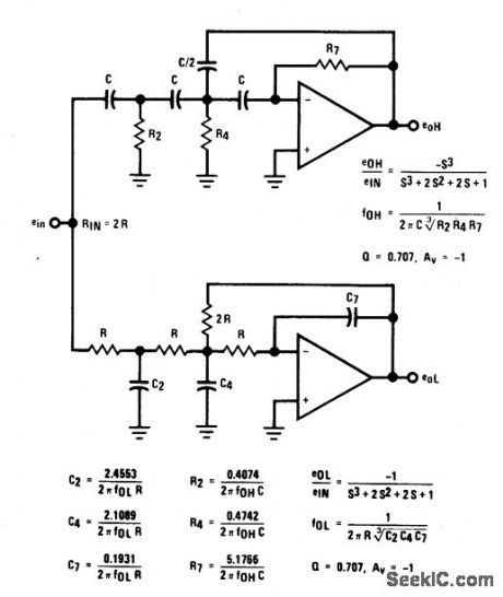
THIRD_ORDER_BUTTERWORTH_CROSSOVER_NETWORK
Published:2009/6/24 20:38:00 Author:Jessie
View full Circuit Diagram | Comments | Reading(1240)
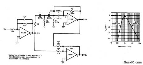
ASYMMETRICAL_THIRD_ORDER_BUTTERWORTH_ACTIVE_CROSSOVER_NETWORK
Published:2009/6/24 20:38:00 Author:Jessie
View full Circuit Diagram | Comments | Reading(1312)
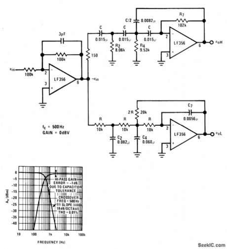
ACTIVE_CROSSOVER_NETWORK
Published:2009/6/24 20:36:00 Author:Jessie
View full Circuit Diagram | Comments | Reading(1469)
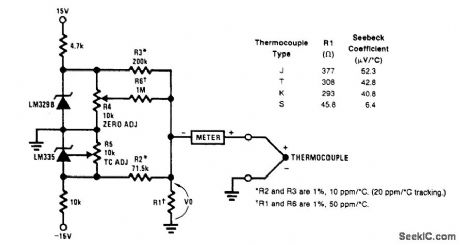
THERMOCOUPLE_COLD_JUNCTION_COMPENSATION
Published:2009/6/24 4:27:00 Author:May
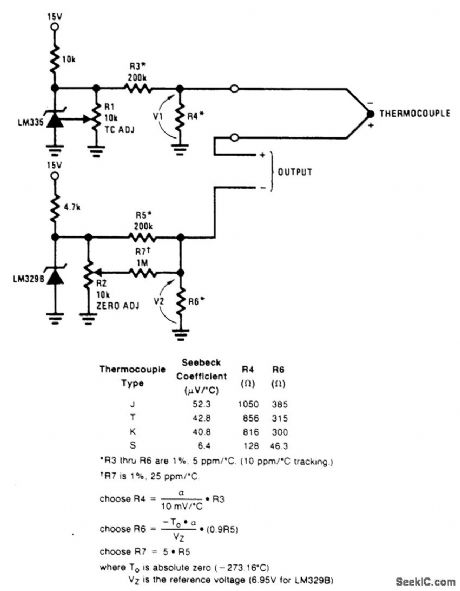
A single-supply circuit is shown. R3 and R4 divide down the 10-mV/°K output of the LM329B and its associated voltage divider provide a voltage to buck out the 0℃ output of the LM335. To calibrate, adjust R1 so that V1 = αT, where cc is the Seebeck coefficient and T is the ambient temperature in degrees Kelvin. Then, adjust R2 so that V1 - V2 is equal to the thermocouple output voltage at the known ambient temperature. (View)
View full Circuit Diagram | Comments | Reading(0)
NATIONAL_SEMICONDUCTOR
Published:2009/6/24 4:05:00 Author:May
A circuit for use with grounded thermocouples is shown. To trim, short out the LM329B and ad-just R5 so that V°= αT, where cc is the Seebeck coefficient of the thermocouple and T is the absolute temperature. Remove the short and adjust R4 so that W equals the thermocouple output voltage at ambient. A good grounding system is essential here, for any ground differential will appear in series with the thermocouple output. (View)
View full Circuit Diagram | Comments | Reading(0)
| Pages:79/126 At 206162636465666768697071727374757677787980Under 20 |
Circuit Categories
power supply circuit
Amplifier Circuit
Basic Circuit
LED and Light Circuit
Sensor Circuit
Signal Processing
Electrical Equipment Circuit
Control Circuit
Remote Control Circuit
A/D-D/A Converter Circuit
Audio Circuit
Measuring and Test Circuit
Communication Circuit
Computer-Related Circuit
555 Circuit
Automotive Circuit
Repairing Circuit