
Electrical Equipment Circuit
Index 62
DARKROOM_EXPOSURE_TIMER
Published:2009/7/24 3:02:00 Author:Jessie


In this circuit, op-amp IC1b and timer IC2 form a voltage-controlled oscillator circuit with its frequency varied by the dual-ganged potentiometer (VR1). Resistor R3 effectively swamps any variations in VR1 value, preventing them from altering the lowest control voltage, as set by R4 and R5. The values of these resistors are chosen to give a ratio between the highest and lowest volt-ages of 32.5:1, which sets the timing range from 0.4 to 13 minutes, ensuring cover of the intended range of 0.5 to 12 minutes. Opamp IC1b is used as a comparator. Capacitor C1 charges in exponential fashion from VR2 and R6 until the voltage across it reaches the selected control voltage from VR1b. When it does so, the output of IC1b goes low, triggering timer IC2, which then delivers a 2.5-ms pulse from output pin 3. This is used to discharge C1 via transistor TR1. VR2 provides the overall trimming adjustment for calibration. From IC2, the output pulses are applied through resistor R10 to the CLOCK input of binary counter IC3. This counts the pulses until the selected output goes high, blocking the CLOCK signal via diode D1. Pin 15 of IC3 is the 11th counter output, so 1024 clock pulses are counted. The final output of the circuit is controlled by quad NOR gate IC4. When the cir-cult is first energized, a positive pulse from C5 via D2 to IC4a pin 1 causes IC4a output pin 3 to go low and IC4b output pin 4 to go high, the OFF state. The high output of IC4b pin 4 charges C4 through R13. When START switch S1 is pressed, output pin 3 goes high, the ON state. At the same time, the pulse resets counter IC3 via its input, pin 11. Capacitor C4 will not be recharged until the output re-turns to the OFF state, ensuring that if switch S1 is held down or accidentally pressed again before timing is complete, the output time will not be affected. Timing ceases when the link-selected output of IC3 goes high and resets IC4a through R14. (View)
View full Circuit Diagram | Comments | Reading(849)
Transformer_driver_for_isolated_RS485_interface
Published:2009/7/24 3:11:00 Author:Jessie
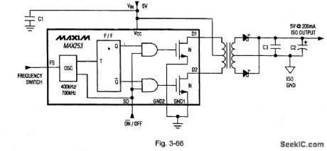
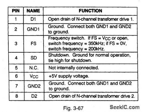
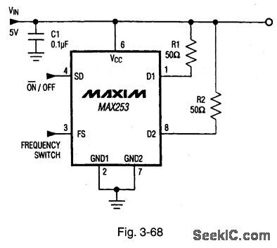
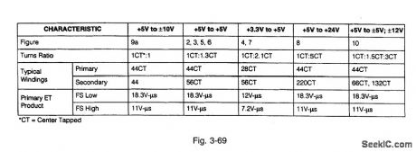
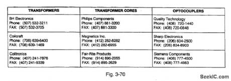
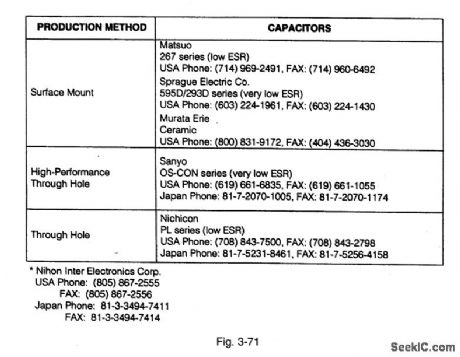


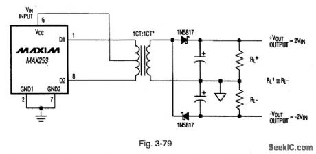
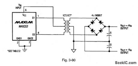

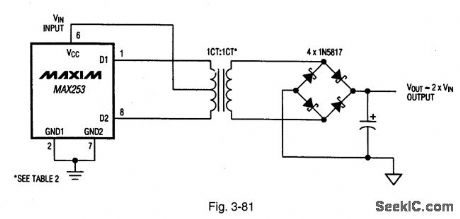
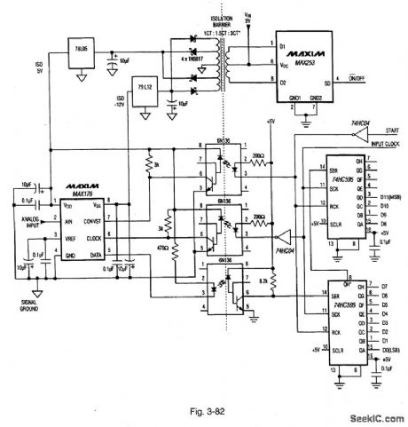
Figures 3-66, 3-67, and 3-68 show the block diagram, pin descriptions, and test circuit for the MAX253. Figures 3-69 through 3-72 show recommended component suppliers. This IC is a monolithic oscillator/driver specifically designed to provide isolated power for an isolated RS485 or RS-232 data interface. The IC drives a center-tapped transformer primary from a 5-V or 3.3-V supply. The secondary can be wound to provide any isolated voltage needed at power levels up to 1 W. The oscillator runs at double the output frequency, driving a toggle flip-flop to ensure a 50% duty cycle to each of the switches. The current is 0.4 μA in shutdown. Figures 3-73 through 3-82 show typical circuits for a variety of applications,MAXIM NEW RELEASES DATA BOOK,1995,P. -125,2-136,2-127,2-128,2-129,2-130,2-131,2-132,2-133,2-134,2-135.
(View)
View full Circuit Diagram | Comments | Reading(2761)
SCR_HORIZONTAL_SWEEP
Published:2009/7/24 3:48:00 Author:Jessie
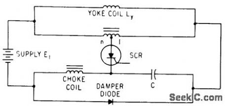
Scr, fired by trigger pulse at start of retrace, transfers to yoke coil the energy stored in 1.27-mfd capacitor C. At end of retrace, energy transfer is completed, damper diode turns on, and energy in yoke returns to supply source E1,giving linear sweep current through yoke. Scr can be General Electric C35, C36, or C40 series. Yoke is 200 mkrohenrys.-T. Tarui, New Deflection Circuit Uses SCR, Saves Power, Electronics, 36:32, p 56-57. (View)
View full Circuit Diagram | Comments | Reading(601)
Low_porter_RS_485_RS_422_transceivers
Published:2009/7/24 3:16:00 Author:Jessie

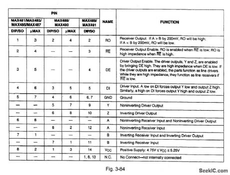
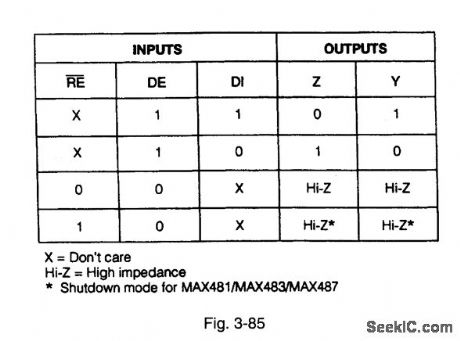
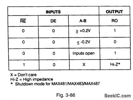
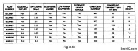
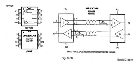
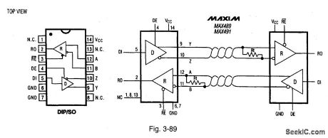
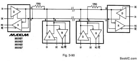
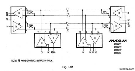

Figure 3-83 shows the typical application circuit and pin configurations for the MAX481/83/85/87. Figures 3-84, 3-85, and 3-86 show the pin functions. Figure 3-87 is the selection table. Figures 3-88 and 3-89 show typical application circuits and pin configurations for the MAX488 through MAX491. Figure 3-90 shows the 1NlAX481/83/85/87 in a typical RS-485 network. Figure 3-91 shows the MAX488 through MAX491 connected in a full-duplex RS485 network. Figure 3-92 shows the MAX488 through MAX491 connected as a line repeater. MAXIM NEW RELEASE DATA BOOK, 1995, P. 2-t59, 2-165, 2-166, 2-167, 2-168, 2-171, 2-172. (View)
View full Circuit Diagram | Comments | Reading(2215)
BOOTSTRAP_SWEEP_FOR_CRO
Published:2009/7/24 3:48:00 Author:Jessie
Hybrid circuit has high linearity and moderate sweep speed,-F. C. Creed, Hybrid Bootstrap Circuits Increase Sweep Linearity, Electronics, 34:31, p 46-48. (View)
View full Circuit Diagram | Comments | Reading(699)
SWEEP_FOR_CURVE_TRACER
Published:2009/7/24 3:43:00 Author:Jessie
Schmitt trig get produces square waves to drive power switch used for obtaining characteristic curves of tunnel diodes in unstable negative-resistance region.-H. G. Dill and M. R. MacPherson, Tracing Tunnel Diode Curves, Electronics, 33:32, p 62-64. (View)
View full Circuit Diagram | Comments | Reading(686)
SLIDE_PROJECTOR_STEPPER_CIRCUIT
Published:2009/7/24 3:26:00 Author:Jessie
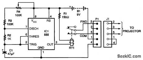
This circuit uses a 555 timer to drive a relay connected to a slide projector to provide automatic advance. R4 sets the time between slide changes. (View)
View full Circuit Diagram | Comments | Reading(1081)
CONSTANT_EXPOSURE_ENLARGER_TIMER_CIRCUIT
Published:2009/7/24 3:25:00 Author:Jessie
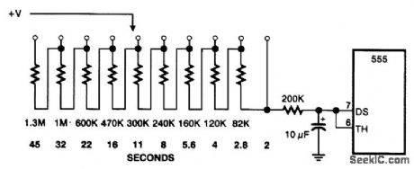
This circuit shows how to set up a NE555 timer to produce time steps proportional to f/stopsShown are values for switch-selected times of 2, 2. 8, 4 5. 6, etc, through 45 s for constant exposure with various enlarger lens settings. (View)
View full Circuit Diagram | Comments | Reading(821)
FAST_800_V_SWEEP
Published:2009/7/24 3:38:00 Author:Jessie

Hybrid bootstrap or arangement with transistors in cascade generates 800-V sweeps in either polarity with 0.15 microsec duration.-F. Q. Creed, Hybrid Bootstrap Circuits Increase Sweep Linearity, Electronics, 34:31, p 46-48. (View)
View full Circuit Diagram | Comments | Reading(649)
TRIGGERED_GROUNDED_GRID
Published:2009/7/24 3:37:00 Author:Jessie

Triggered linear sawtooth generator uses grounded-grid amplifier, eliminating initial step voltage that usually occurs in Miller sweep.-C. Sing, Grounded-Grid Circuit Sweeps Better Than Miller or Bootstrap, Electronics, 38;6, p 83-84. (View)
View full Circuit Diagram | Comments | Reading(676)
TWO_TRANSISTOR_PHANTASTRON_SWEEP
Published:2009/7/24 3:36:00 Author:Jessie
Combined positive and negative feedback loops in two. transistor circuit give phantastron effect of single pentode with good sweep linearity.-A. S. Kislovsky, Sweep Circuits Using Two Three-Terminal Active Elements, Electronics, 35:12, p 54-55. (View)
View full Circuit Diagram | Comments | Reading(957)
SHF_SWEEP_GENERATOR
Published:2009/7/24 3:36:00 Author:Jessie
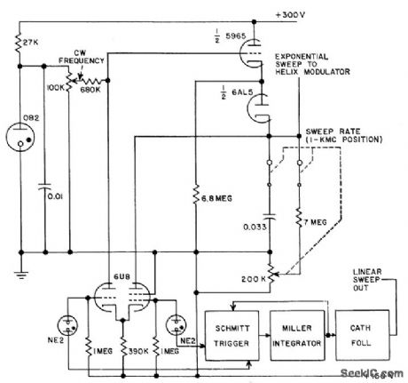
Swept-frequency signal source using backward-wove oscillator tube offers variable sweep rate in microwave region between 8,200 and 12,400 Mc. Sweep width is continually adjustable from 3 Mc to 4,200 Mc. May be modulated with either f-m or a-m.-D. E. Wheeler and P. D. Lacy, SHF Frequency Sweeper Uses Backward-Wave Tube, Electronics, 31:1, p 76-78. (View)
View full Circuit Diagram | Comments | Reading(892)
HIGH_SPEED_HYBRID_BOOTSTRAP
Published:2009/7/24 3:35:00 Author:Jessie
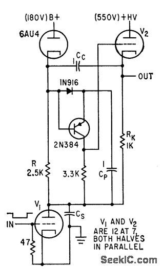
Speed is increased because Cc does not have to supply charging current for Cs, but only current re quired by grid leak resistor; this is small, so Cc can be small und easily recharged during quiescent period.-F. C. Creed, Hybrid Bootstrap Circuits Increase Sweep linearity, Electronics, 34:31, p 46-48. (View)
View full Circuit Diagram | Comments | Reading(619)
BiMOS_LED_bar_graph_driver
Published:2009/7/24 4:50:00 Author:Jessie
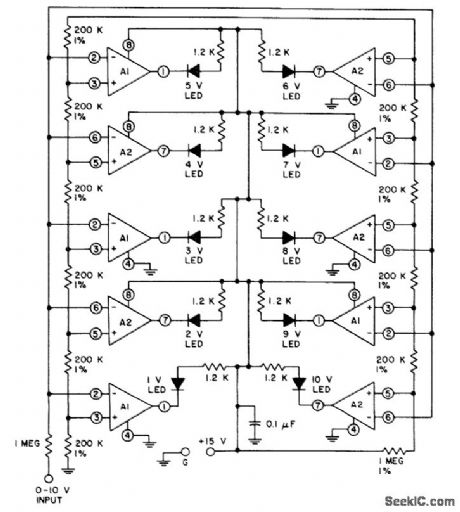
Fig. 15-31 In this circuit, the LED for a particular comparator is turned on when the input voltage reaches the voltage on the resistor-driver reference.Because of the MOSFET input(and bipolar output)this circuit is ideal where input-signal loading is critical-even though many comparator inputs are driven In parallel.Figures 15-30B and 15-30C show the pin connections and electrical characteristics, respectively. Harris Semiconductor Linear&Telecom IC. 1991, p. 4-23. (View)
View full Circuit Diagram | Comments | Reading(947)
BiMOS_window_comparator
Published:2009/7/24 4:50:00 Author:Jessie

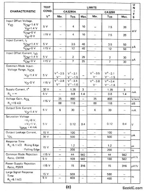
Fig. 15-30 In this circuit, the LED is turned on whenever the input signal is above the lower limit (VL) but below the upper limit (VU), as determined by the R1/R2/R3 divider. Figures 15-30B and 15-30C show the pin connections and electrical characteristics, respectively. Harris Semiconductor Linear & Telecom ICs, 1991 p 4-15, 4 18 4-22. (View)
View full Circuit Diagram | Comments | Reading(631)
STEREO_TV_DECODER
Published:2009/7/1 20:28:00 Author:May

The composite input signal is preamplified by transistor Q1 and is then coupled to the high-pass filter composed of C3, C4, R6, and R7. The filtered audio is then passed to IC1, an MC1310P Coilless Stereo Demodulator. That IC is normally used to demodulate broadcast-band FM signals, but by changing the frequency of its on-board VCO (Voltage Controlled Oscillator) slightly (from 19 kHz to 15.734 kHz), we can use that IC to detect stereo-TV signals. A block diagram of the MC1310P is shown in Fig.22-5. Notice that the components connected to pin 14 control the VCO's frequency, hence the pilot-detect and carrier frequencies. For use in an FM receiver, the VCO would run at four times the 19 kHz pilot frequency (76 kHz), but for our application, it will run at four times the 15.734 kHz pilot frequency of stereo TV, or 62.936 kHz. The MC1310P divides the master VCO signal by two in order to supply the 31.468 kHz carrier that is used to detect the L - R audio signal. The L - R signal undergoes normal FM detection, and at that point we've got two audio signals: L + R and L - R. The decoder block in the IC performs the addition and subtraction to produce the separate left and right signals. R10and C10 form a de-emphasis network that compensates for the 75μs pre-emphasis that the left channel underwent; R12 and C11 perform the same function for the right channel. (View)
View full Circuit Diagram | Comments | Reading(0)
TRANSISTORS_SIMULATE_PHANTASTRON
Published:2009/7/24 3:34:00 Author:Jessie
Three transistors simulate current-partitioning action of pentode vacuum-tube phantastron sawtooth sweep generator. Potentiometer in bias and feedback circuit can be adjosted for either triggered or free-running phantastron sweep.-N. C. Hekimian, Phantastron Circuits Using Transistors, Electronics, 34:8, p 46-47. (View)
View full Circuit Diagram | Comments | Reading(750)
KLYSTRON_SWEEP
Published:2009/7/24 3:34:00 Author:Jessie
Provides sweep voltage for klystron in microwave interferometer system, plus vertical sweep end trigger for oscilloscope.-H. L. Bunn, Determining Electron Density und Distribution in Plasmas, Electronics, 34:14, p 71-75. (View)
View full Circuit Diagram | Comments | Reading(956)
CONSTANT_AMPLITUDE_FOR_THREE_RANGES
Published:2009/7/24 3:32:00 Author:Jessie

Multiple-range sweep generator for airborne radar provides constant-amplitude out put sawtooth, along with fast-rising gate pulse or pedestal having duration of saw tooth. linearity is kept within 1% without using bootstrap.-H. P. Brockman, Sweep Generator Design: How to Keep It Simple, Electronics, 33:3, p 92. (View)
View full Circuit Diagram | Comments | Reading(900)
TRIODE_PHANTASTRON_SWEEP
Published:2009/7/24 3:42:00 Author:Jessie
Active elements V1-V2 serve with isolation diode V3 to give action of single pentode with good sweep linearity.-A. S. Kislovsky, Sweep Circuits Using Two Three-Terminal Active Elements, Electronics, 35:12, p 54-55. (View)
View full Circuit Diagram | Comments | Reading(722)
| Pages:62/126 At 206162636465666768697071727374757677787980Under 20 |
Circuit Categories
power supply circuit
Amplifier Circuit
Basic Circuit
LED and Light Circuit
Sensor Circuit
Signal Processing
Electrical Equipment Circuit
Control Circuit
Remote Control Circuit
A/D-D/A Converter Circuit
Audio Circuit
Measuring and Test Circuit
Communication Circuit
Computer-Related Circuit
555 Circuit
Automotive Circuit
Repairing Circuit