
Electrical Equipment Circuit
Index 70
IC_VCO_with_sawtooth_and_pulse_outputs
Published:2009/7/25 4:11:00 Author:Jessie

This circuit is similar to that of Fig. 5-36, except that simultaneous triangle and square outputs are available. The duty cycle of the outputs is controlled by R2/R3, while the frequency is set by C, R2/R3, as shown by the equations. See Conditions in Fig. 5-36B. (View)
View full Circuit Diagram | Comments | Reading(806)
_5_V_from___5_V_at_mediurn_power_lowo_noise_
Published:2009/7/25 4:10:00 Author:Jessie
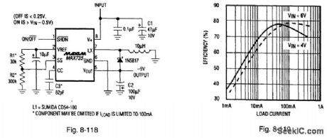
Figure 8-118 shows a MAX735 PWM regulator connected to provide -5 V at medium power. Figure 8-119 shows the efficiency curves. The input voltage range is 4 V to 6.2 V, with a quiescent current of 1.6 mA (VIN = 5 V), a maximum load current of 200 mA (VIN = 5 V), and a shutdown current of 10 μA. MAXIM BATTERY MANAGEMENT CIRCUIT COLLECTION, 1994, P. 58. (View)
View full Circuit Diagram | Comments | Reading(666)
IC_function_generator_connected_for_sine_output_without_external_adjustment
Published:2009/7/25 3:58:00 Author:Jessie
This circuit is similar to that of Fig. 5-31, except that the circuit is connected for sine outputs (S1 closed). R1 at pin 7 provides frequency tuning. Output swing is greater than V+/2, and typical distortion (THD) is less than 2.5%.If lower sine distortion is desired, use Fig. 5-33. If a triangle output is desired, open S1. The circuit can be used with a split supply by replacing all ground connections with V-, and connect R3 to ground (View)
View full Circuit Diagram | Comments | Reading(893)
Basic_IC_function_generator
Published:2009/7/25 3:57:00 Author:Jessie
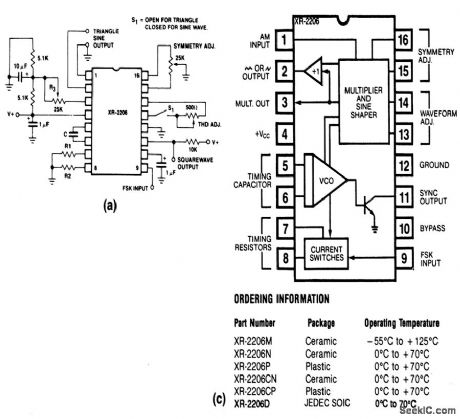
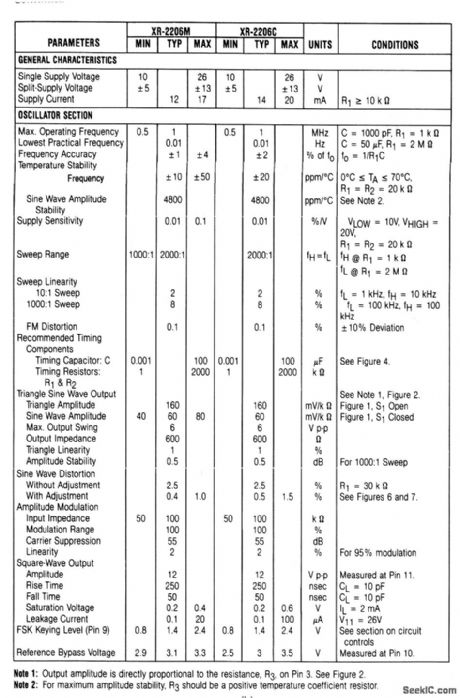
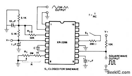
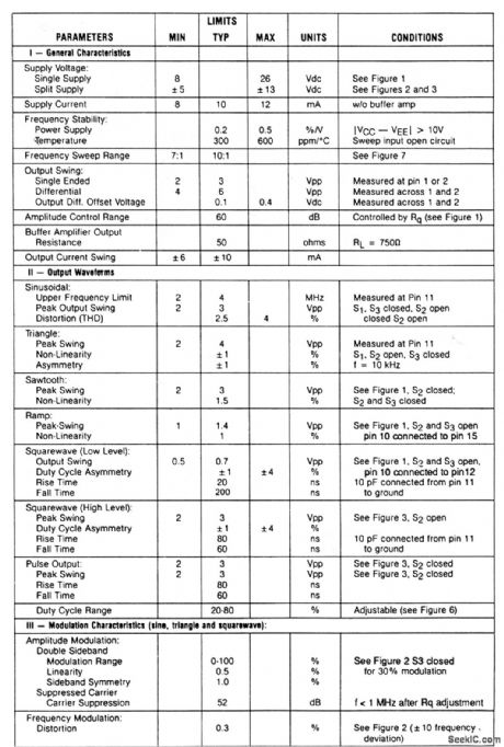
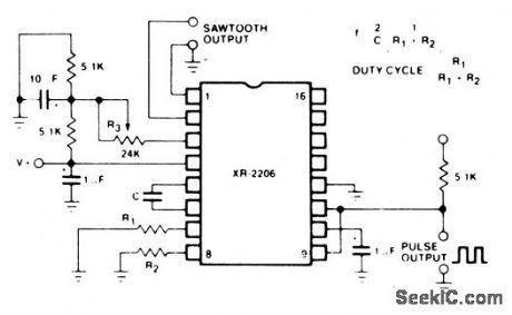
This circuit uses an XR-2206 to provide sine,square,triangle,ramp and pulse output waveforms, which can be both amplitude and frequency modulated Electrical characteristics and functional circuits of the XR-2206 are shown in Figs 5-31B and C, respectively, The operating frequency is set by capacitor C between puts 5 and 6.The THD ADJ pot between pins 13 and 14 adjusts the waveform.R3 sets the amplitude(Fig.5-31D)The SYMMETRY ADJ pot between pins 15 and 16 is a fine waveform adjustment.Open S1 for triangle, close S1 for sine.The square output is at pin 11 .See Conditions in Fig. 5-31B (View)
View full Circuit Diagram | Comments | Reading(4102)
IC_waveform_generator_for_high_level_pulse_and_square_wave_output
Published:2009/7/25 3:54:00 Author:Jessie
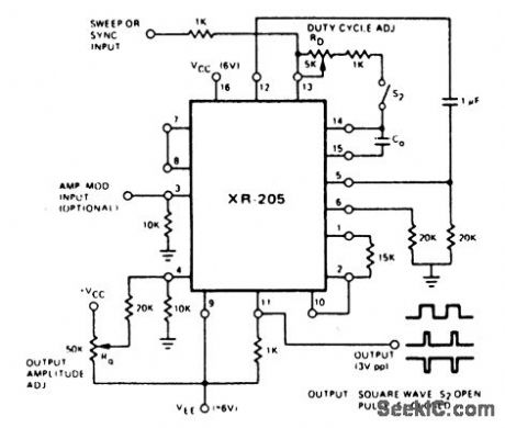
This circuit is similar to that of Fig. 5-28, except the circuit provides high-level pulse (S2 closed) or square (S2 open) outputs. Duty cycle of the pulse is controlled by RD. The amplitude and polarity of either pulse or square output is controlled by Rq. See Conditions in Fig. 5-28B. (View)
View full Circuit Diagram | Comments | Reading(789)
IC_waveform_generator_with_split_supply_and_AM_FM_modulation_output
Published:2009/7/25 3:52:00 Author:Jessie

This circuit is similar to that of Fig. 5-28, except that the circuit is operated from a split-supply and provides for AM modulation at pin 3, or FM modulation at pin 13. See Conditions in Fig. 5-28B. (View)
View full Circuit Diagram | Comments | Reading(996)
Basic_IC_waveform_generator
Published:2009/7/25 3:52:00 Author:Jessie
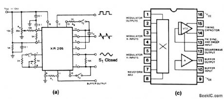
This circuit uses an XR-205 to provide sine, square, triangle, ramp and sawtooth output waveforms, which can be both amplitude and frequency modulated. Electrical characteristics and functional circuits of the XR-205 are shown in Figs. 5-28B and 5-28C, respectively. The operating frequency is set by capacitor Co between pins 14 and 15. With the sweep input open-circuited, the output frequency: f0 (in Hz) =400/C0 (inμF). The Rj pot between pins 7 and 8 adjusts the waveform. The Rq, pot at pin 4 sets the amplitude. For a triangle output at pins 1 and 2 (or pin 11 if the internal buffer is used), both S1 and S2 are open and S3 is closed. For a sine output, open S2, close S1 and S3, adjust Rj for minimum harmonic distortion, and Rq for a maximum output of about ± 3 Vpp. For a sawtooth output, open S1, close S2/S3. For a ramp output at pin 11 (of about 1.4 Vpp) open S3. The ramp duty cycle is controlled by RB across pins 13-14 or 13-15 (duty cycle decreases as RB is decreased). See Conditions in Fig. 5-28B. (View)
View full Circuit Diagram | Comments | Reading(2477)
Low_distortion_oscillator
Published:2009/7/25 3:47:00 Author:Jessie
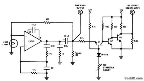
This circuit provides in-phase sine and TTL outputs at 1 kHz, with 1/4-W output drive. The symmetry-adjust pot is trimmed so that the edges of the TTL output precisely line up with the zero crossing of the sine output. (View)
View full Circuit Diagram | Comments | Reading(0)
Tuning_fork_stabilized_frequency_standard
Published:2009/7/25 3:46:00 Author:Jessie
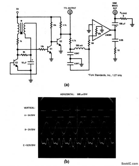
This circuit provides both sine and TTL outputs, operates from 5V with low power consumption. Figure 5-26B shows typical waveforms.Trace C is the output of a distortion analyzer connected to the sine output (with has less than 1% distortion, and will drive an 8-Ω load). (View)
View full Circuit Diagram | Comments | Reading(735)
Portable_oscilloscope_calibrator
Published:2009/7/25 3:46:00 Author:Jessie
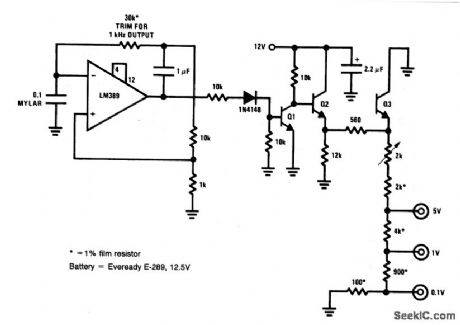
This circuit allows a quick check of oscilloscope time-base and vertical calibration. The circuit can be built into a small hand-held box and powered by a 12.5-V battery, as shown. The 30-kΩ resistor should be trimmed for a precise (15 Hz) 1-kHz output using a frequency counter. Accuracy of the 0.1-V, 1-V, and 5-V outputs depends on adjustment of the 2-kΩ pot, and the precision of the fixed resistors. (View)
View full Circuit Diagram | Comments | Reading(1436)
IC_VCO_with_alternate_frequency_sweep_operation
Published:2009/7/25 4:10:00 Author:Jessie
This circuit is an alternate to that of Fig. 5-50, but operates only with negative values of VC. If VC goes to 0 or above, pin 7 is deactivated, and frequency is fixed at 1/(R3C). (View)
View full Circuit Diagram | Comments | Reading(674)
IC_VCO_with_frequency_sweep_operation
Published:2009/7/25 4:09:00 Author:Jessie
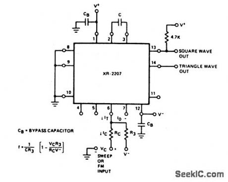
This circuit is similar to that of Fig. 5-36, except that the triangle and square outputs are controlled by a sweep or FM input. The frequency is determined by C, R3, RC, VC, and V- as shown by the equations. (View)
View full Circuit Diagram | Comments | Reading(639)
_5_V_from__5_V_or_five_to_eight_cells
Published:2009/7/25 4:09:00 Author:Jessie
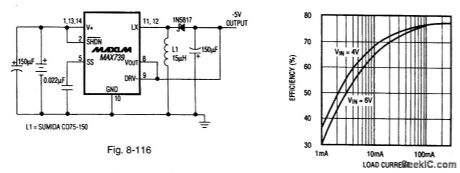
Figure 8-116 shows a MAX739 PWM regulator connected to provide -5 V from a five- to eight-cell battery (or a fixed +5-V source). Figure 8-117 shows the efficiency curves. The input voltage range is 3.8 V to 11 V, with a no-load start-up of 4 V maximum, a quiescent current of 1.8 mA (VIN = 5 V), a maximum load current of 200 mA (VIN =5 V), and a 1-μA shutdown current. MAXIM BATTERY MANAGEMENT CIRCUIT COLLECTION, 1994, P. 57. (View)
View full Circuit Diagram | Comments | Reading(627)
IC_VCO_with_single_supply_and_fixed_frequency
Published:2009/7/25 4:07:00 Author:Jessie
This circuit is similar to that of Fig. 5-36, except that a single supply is used, and the output is at a fixed frequency, determined by R3 and C, as shown by the equations. (View)
View full Circuit Diagram | Comments | Reading(694)
IC_VCO_with_split_supply_and_fixed_frequency
Published:2009/7/25 4:07:00 Author:Jessie
This circuit is similar to that of Fig. 5-36, except that a split supply is used, and the output is at a fixed frequency, determined by R3 and C as shown by the equations. (View)
View full Circuit Diagram | Comments | Reading(606)
_5_V_from___5_Vor_four_to_eight_cells
Published:2009/7/25 4:06:00 Author:Jessie
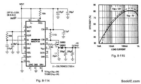

Figure 8-114 shows a MAX714 PWM regulator connected to provide-5 V from a four- to eight-cell battery (or a fixed +5-V Source). Figure 8-115 shows theefficiency curves. The input voltage range is 4 V to 15 V, with a quiescent current of 3 mA (VIN =5 V), a maximum load current of 1 A(VIN =4.75 V), and 1.25 A (VIN=12V), and a shutdown current of 30 μA. MAXIM BATTERY MANAGEMENT CIRCUIT COLLECTION. 1994, P. 56.
(View)
View full Circuit Diagram | Comments | Reading(675)
IC_VCO_voltrtge_controlled_oscillcltor_with_single_supply
Published:2009/7/25 4:05:00 Author:Jessie
This circuit is similar to that of Fig. 5-36, except that a single supply is used. (View)
View full Circuit Diagram | Comments | Reading(644)
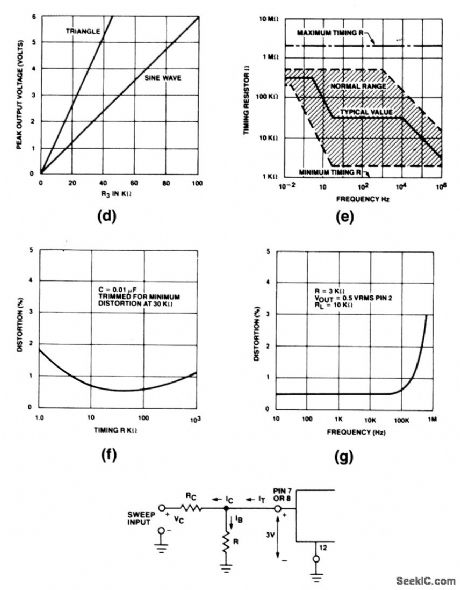
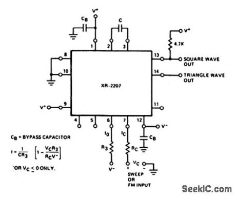
IC_VCO_voltrtge_controlled_oscillator_with_split_supply
Published:2009/7/25 4:05:00 Author:Jessie
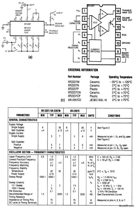
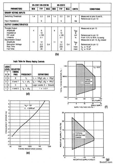
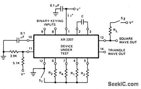
This circuit uses an XR-2207 to provide simultaneous triangle and square outputs (with binary keying if desired) over a frequency range of 0.01 Hz to 1 MHz, with a typical drift of 10 ppm/°C. The output can be linearly swept over a 1000:1 range with an external control voltage. Both the triangle and square output duty cycle can be varied from 0.1% to 99.9%. Electrical characteristics and functional circuits of the XR-2207 are shown in Figs. 5-36B and 5-36C, respectively. Operating frequency is set by capacitor C between pins 2 and 3, and timing resistors at pins 4-7. See Conditions in Fig. 5-36B. (View)
View full Circuit Diagram | Comments | Reading(702)
_5_V_from_a_negcttive_input_voltage
Published:2009/7/25 4:03:00 Author:Jessie
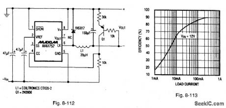
Figure 8-112 shows a MAX752 step-up regulator connected to provide a +5-V output from a 6-V to -15-V input (six- to eight-cell battery). Quiescent current with a VIN of -6 V is 1.5 mA, and maximum load current with a VIN of -6 V is 500 mA. Figure 8-113 shows the efficiency curves. The circuit works only in situations where the negative battery terminal need not be tied to ground (in systems that do not require multiple-output voltages taken from the battery). MAXIM BATTERY MANAGEMENT CIRCUIT COLLECTION, 1994, P. 3 (View)
View full Circuit Diagram | Comments | Reading(594)
IC_function_generator_connected_for_pulse_and_ramp_outputs
Published:2009/7/25 4:01:00 Author:Jessie
This circuit is similar to that of Fig. 5-31, except that the XR-2206 is connected for pulse and ramp outputs. In this mode, the FSK keying terminal (pin 9) is shorted to the square output (pin 11), and the IC automatically frequency-shift keys itself between two separate frequencies during the positive-going and negative-going output waveforms. The pulse width and duty cycle can be adjusted from 1% to 99% by selection of R1 and R2, using the equations. The values of R1 and R2 should be in the range of 1 kΩ to 2 MΩ. (View)
View full Circuit Diagram | Comments | Reading(2531)
| Pages:70/126 At 206162636465666768697071727374757677787980Under 20 |
Circuit Categories
power supply circuit
Amplifier Circuit
Basic Circuit
LED and Light Circuit
Sensor Circuit
Signal Processing
Electrical Equipment Circuit
Control Circuit
Remote Control Circuit
A/D-D/A Converter Circuit
Audio Circuit
Measuring and Test Circuit
Communication Circuit
Computer-Related Circuit
555 Circuit
Automotive Circuit
Repairing Circuit