
Electrical Equipment Circuit
Index 69
Precision_VCO
Published:2009/7/25 3:21:00 Author:Jessie
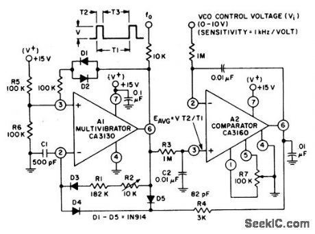
This voltage-controlled oscillator operates with a tracking error in the order of 0.02%、and a temperature coefficient of 0.01%/℃.Adjust both R2 and R7 for an output sensitivity of 1-kHz/V(from 0-to 10-V input) (View)
View full Circuit Diagram | Comments | Reading(829)
Function_generator_with_wide_tuning_range
Published:2009/7/25 3:19:00 Author:Jessie
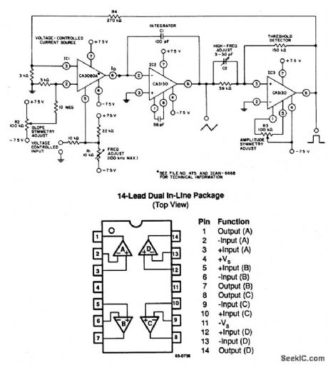
The adjustment range of this generator is in excess of 1,000,000/1, using a single frequency-adjust potentiometer, or an external voltage-control source.Both the pulse amplitude and triangle-wave slope symmetry can be adjusted individually. (View)
View full Circuit Diagram | Comments | Reading(1)
Voltage_controlled_sine_wave_oscillator
Published:2009/7/25 3:18:00 Author:Jessie
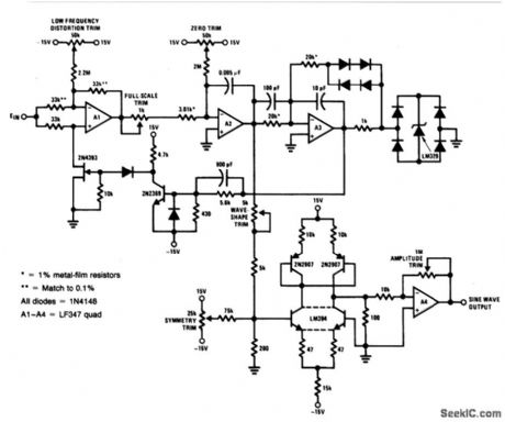
For a 0- to 10-V input, this circuit produces sine-wave outputs of 1 Hz to 20 kHz, with better than 0.2% linearity. Distortion is about 0.4% and the sine-wave output frequency and amplitude settle instantaneously to a step-input change. To calibrate, apply 10 V to the input and adjust the wave-shape trim and symmetry trim for minimum distortion on a distortion analyzer. Next, adjust the input voltage for an output frequency of 10 Hz and trim the low-frequency distortion for minimum indication on the distortion analyzer. Finally, alternately adjust the zero and full-scale pots so that inputs of 500μV and 10 V yield respective outputs of 1 Hz and 20 kHz. (View)
View full Circuit Diagram | Comments | Reading(2179)
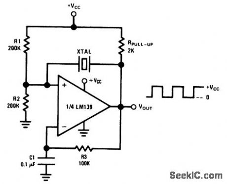
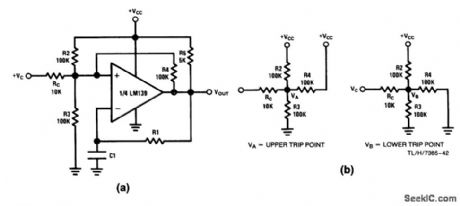
Crystal_controlled_square_wave_oscillator
Published:2009/7/25 3:17:00 Author:Jessie
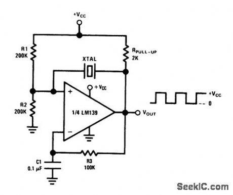
In this circuit, the values of R1 and R2 are equal so that the LM139 comparator switches symmetrically about +Vcc/2. To ensure a 50% duty cycle, the RC time constant of R3 and C1 is set to be several times greater than the period of the oscillating frequency (which depends on the crystal resonant frequency).When specifying the crystal, order series-resonant, along with the desired temperature coefficient and load capacitances to be used.
(View)
View full Circuit Diagram | Comments | Reading(1394)
Pulse_generator_with_variable_duty_cycle
Published:2009/7/25 3:15:00 Author:Jessie
In this circuit, time t1 (pulse width) is set by R4, while time t2 (frequency) is set by R5. 1N914 or equivalent diodes can be used and D2. (View)
View full Circuit Diagram | Comments | Reading(0)
50_MHz_trigger
Published:2009/7/25 3:13:00 Author:Jessie
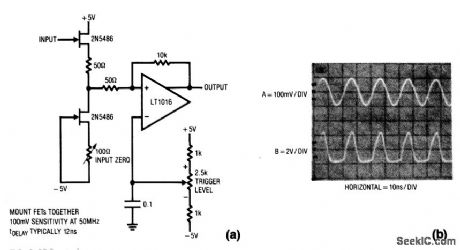
In this circuit, the FETs form a simple high-speed buffer and the LT1016 compares the buffer output to the voltage set by the trigger-level pot. The circuit has a 100-mV sensitivity at 50 MHz. Figure 5-2B shows the trigger response (trace B) to a 50-MHz sine wave (trace A). To calibrate, ground the input and adjust the input-zero control for 0 V at the Q2 drain terminal. (View)
View full Circuit Diagram | Comments | Reading(1698)
_5_V_from_a_charge_pump_low_power
Published:2009/7/25 4:16:00 Author:Jessie
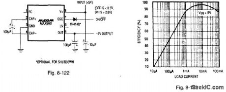
Figure 8-122 shows a MAX660 charge pump connected to provide -5 V at low power. Figure 8-123 shows the efficiency curve. The input voltage range is 1.5 V to 5.5 V, output impedance is 6.5 (1, quiescent current is 100 μA (VIN = 5 V). maximum load current is 100 mA (VIN = 4.75 V), and shutdown current is 10 μA. The circuit is low noise, with a fixed-frequency oscillation (between 10 and 45 kHz), and with an unregulated output (output voltage follows input variations). MAXIM BATTERY MANAGEMENT CIRCUIT COLLECTION, 1994, P. 60.
(View)
View full Circuit Diagram | Comments | Reading(635)
IC_precision_oscillator
Published:2009/7/25 4:15:00 Author:Jessie
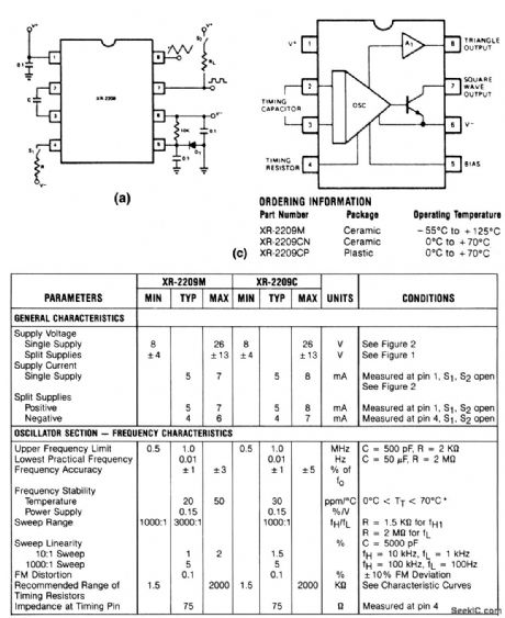

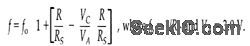
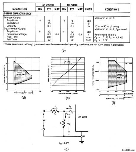
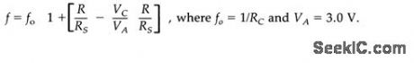
This circuit uses an XR-2209 to provide simultaneous triangle and square outputs over a frequency range of 0.01 Hz to 1 MHz, with a typical drift of 20 ppm/℃. The output can be swept over a 1000:1 range with an external control voltage. Electrical characteristics and functional circuits of the XR-2209 are shown in Figs. 5-44B and 5-44C, respectively. Operating frequency is set by capacitor C between pins 2 and 3, and the timing resistor at pin 4. Use a 1N4148 or equivalent for D1. See Conditions in Fig. 5-44B. Figure 5-44G shows connections for frequency-sweep operation. The frequency of such operation is determined by: (View)
View full Circuit Diagram | Comments | Reading(905)
Wide_range_function_generator
Published:2009/7/25 3:44:00 Author:Jessie
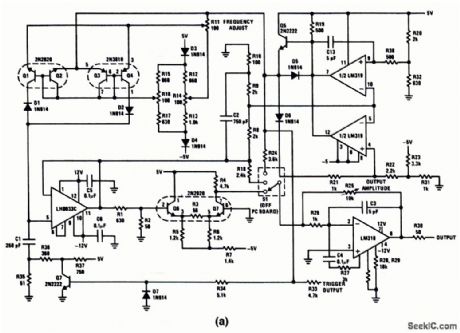
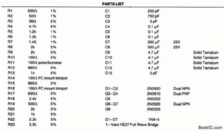
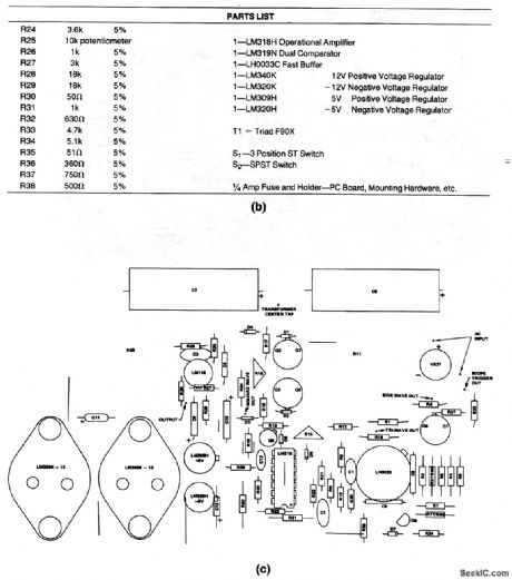
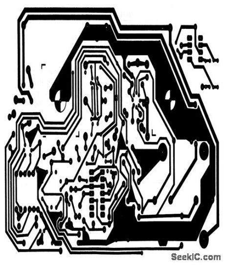
This circuit produces all three waveforms(sine, triangle, square)as selected by S1、at frequencies from 10 Hz to 1 MHz,Output amplitude is set by R25 Output frequency is set by R11.Figures 5-24B, 5-24C, 5-24D、and show parts list, recommended component location, PC layout and Power supply, respectively. To calibrate, set R11 for 1-MHz output and adjust R16 for proper output symmetry.Then,set R11 for 10 Hz and adjust R14 for good symmetry. (View)
View full Circuit Diagram | Comments | Reading(0)
CMOS_staircase_generator
Published:2009/7/25 3:40:00 Author:Jessie
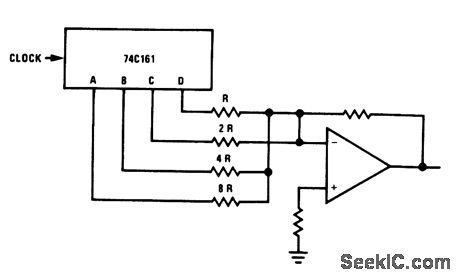
This circuit uses a 74C161 and any suitable op amp (such as an LM301) to form a staircase generator. Linearity of the staircase depends on precision of the resistors. (View)
View full Circuit Diagram | Comments | Reading(1215)
CMOS_one_shot
Published:2009/7/25 3:39:00 Author:Jessie
This circuit uses two sections ofan MM74C02 to form a one-shot. (View)
View full Circuit Diagram | Comments | Reading(844)
CMOS_square_wave_generator
Published:2009/7/25 3:38:00 Author:Jessie
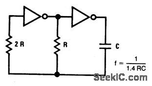
This circuit uses two sections of an MM74C04 to form a square-wave oscillator. (View)
View full Circuit Diagram | Comments | Reading(744)
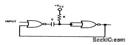
CMOS_phase_shift_oscillator
Published:2009/7/25 3:37:00 Author:Jessie
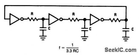
This circuit uses three sections of an MM74C04 to form a phase shift oscillator. (View)
View full Circuit Diagram | Comments | Reading(653)
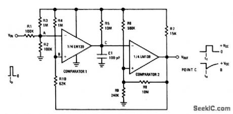
Pulse_width_modulator
Published:2009/7/25 3:37:00 Author:Jessie
With this circuit, the values of R1 and C1 can be varied to produce any desired center frequency from less than 1 Hz to the maximum frequency of the LM139 comparator (which will be limited by + VCC and the output slew rate). The duty cycle of the output square wave is altered if the input control voltage is moved above or below ground, because the change in control voltage alters the comparator trip points. These trip points can be found if the circuit is simplified, as shown in Fig. 5-19B. (View)
View full Circuit Diagram | Comments | Reading(1)
Bistable_multivibrator
Published:2009/7/25 3:35:00 Author:Jessie

With this circuit, a pulse at the SET input causes the output to go high.A pulse at the RESET input pulls the output low. If both Q and Q outputs are needed, another LM139 comparator can be added (as shown in dashed lines). (View)
View full Circuit Diagram | Comments | Reading(0)
Multivibrator_with_input_lock_out
Published:2009/7/25 3:34:00 Author:Jessie
With this circuit, pulse width is independent of supply voltage, and a 99% duty cycle is possible. Input trigger amplitude is set by R1, R2, R3, R4, and R10. When triggered, the output is high, causing the voltage at the noninverting input of comparator 1 to go to +VCC. This prevents any additional input pulses from disturbing the circuit until the output pulse has been completed. Pulse width is set by R6, R9, and C1. (View)
View full Circuit Diagram | Comments | Reading(675)
One_shot_multivibrator
Published:2009/7/25 3:32:00 Author:Jessie
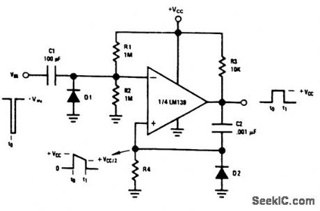
This simple one-shot multivibrator uses one section of an LM139 comparator.Output pulse width is set by C2/R4.Input trigger amplitude is set by R1/R2. (View)
View full Circuit Diagram | Comments | Reading(0)
Alternate_lovo_frequency_sine_wave_generator
Published:2009/7/25 3:32:00 Author:Jessie
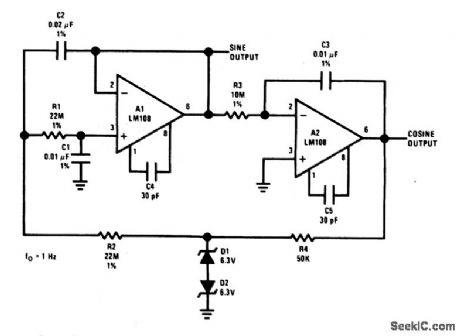
Compare this circuit (which requires two LM108s) to that of Fig.5-11. (View)
View full Circuit Diagram | Comments | Reading(648)
_5_V_from__5_V_at_low_power
Published:2009/7/25 4:13:00 Author:Jessie
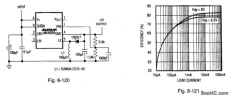
Figure 8-120 shows a MAX639 PFM regulator connected to provide -5 V at low power. Figure 8:121 shows the efficiency curves. The input voltage range is 1.2 V to 6 V, with a no-load start-up of 1 V, a quiescent current of 35 μA (VIN = 5 V), a maximum load current of 80 mA (VIN = 4.75 V), and a shutdown current of 10 μA. MAXIM BATTERY MANAGEMENT CIRCUIT COLLECTION, 1994, P. 59. (View)
View full Circuit Diagram | Comments | Reading(628)
IC_VCO_with_multi_channel_FSK_operation
Published:2009/7/25 4:12:00 Author:Jessie
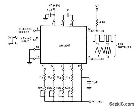
This circuit is similar to that of Fig.5-36.except that the XR-2207 is connected for square and triangle FSK outputs,Mark and space frequencies f1 and f2 are selected by the choice of R1 through R3 and C,as shown by the equations of Fig.5-36D The keying signal is applied at pin 9.If only a single FSK channel is used connect pin 8 to V+or ground, and omit the remaining timing resistors.Notice that f1 and f2 can be fine tuned using the pots. Set f1 first with pin 9 low.Because frequency stability is related directly to the timing components, use parts with low Tc. Typical drift for 0℃ to 75℃ is± 0.2%. (View)
View full Circuit Diagram | Comments | Reading(1119)
| Pages:69/126 At 206162636465666768697071727374757677787980Under 20 |
Circuit Categories
power supply circuit
Amplifier Circuit
Basic Circuit
LED and Light Circuit
Sensor Circuit
Signal Processing
Electrical Equipment Circuit
Control Circuit
Remote Control Circuit
A/D-D/A Converter Circuit
Audio Circuit
Measuring and Test Circuit
Communication Circuit
Computer-Related Circuit
555 Circuit
Automotive Circuit
Repairing Circuit