
Electrical Equipment Circuit
Index 66
Op_amp_full_wave_rectifier
Published:2009/7/24 21:51:00 Author:Jessie
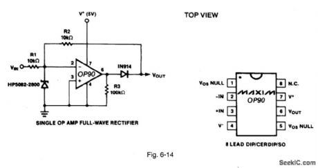
Figure 6-14 shows an OP90 connected to form a full-wave rectifier. This is similar to the circuit of Fig. 6-6, except that the OP90 has a maximum input-offset voltage of 150-μV (higher than the maximum of 70 μV for the MAX480). Similarly, the input bias current, input offset current, and drift specifications of the OP90 are higher than the MAX480. MAXIM NEW RELEASES DATA BOOK, 1993, P. 3-69. (View)
View full Circuit Diagram | Comments | Reading(1746)
Low_noise_microphone_preamplifier
Published:2009/7/24 21:50:00 Author:Jessie

Figure 6-13 shows an OP27 connected as a low-noise microphone preamp. The input voltage noise is 3 nV√Hz at 1 kHz. The OP27 has an 8-MHz gain-bandwidth product and a 2.8-V/μs slew rate. The OP37 has a 63-MHz gain-bandwidth with a 17-V/μs slew rate. Input-offset voltage is 10 μV, drift is 0.2 μV/℃, and output swing is ±10 V into 600 Ω. MAXIM NEW RELEASES DATA BOOK, 1993, P. 3-67. (View)
View full Circuit Diagram | Comments | Reading(169)
High_power_booster
Published:2009/7/24 21:10:00 Author:Jessie

Figure 5-39 is a 1-A version of the Fig. 5-36 circuit. Figure 5-40 shows the waveforms for a 10-V negative input step (trace A) with a 10-Ω, load. The amplifier responds (trace B) driving the booster to close the loop. The booster output, lagging by nanoseconds (trace C), drives the load with only minor peaking (which can be minimized with the feedback capacitance trimmer). LINEAR TECHNOLOGY, APPLICATION NOTE 47, P. 47. (View)
View full Circuit Diagram | Comments | Reading(1001)
Single_op_amp_full_wave_rectifier
Published:2009/7/24 21:37:00 Author:Jessie
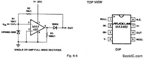
Figure 6-6 shows a MAX480 connected to form a full-wave rectifier. Maximum offset-voltage drift is 1.5 μV/℃, maximum supply current is 20 μA, minimum output drive is 5 mA, maximum input-offset voltage is 70 μV, maximum input bias current is 3 nA, and minimum open-loop gain is 700 V/mV. MAXIM NEW RELEASES DATA BOOK, 1993, P. 3-23. (View)
View full Circuit Diagram | Comments | Reading(0)
Op_amp_function_generator
Published:2009/7/24 21:36:00 Author:Jessie
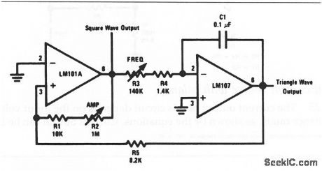
This circuit is the op-amp version of the classic sine/triangle function generator (chapter 5). Notice that both frequency and amplitude are adjustable. (View)
View full Circuit Diagram | Comments | Reading(1897)
Multiplexed_cable_driver_2_channel
Published:2009/7/24 21:34:00 Author:Jessie

Figure 6-4 shows a multiplexer/amplifier MAX442 connected to provide 2 channels of video signal to a single cable. Unity-gain bandwidth is 140 MHz, channel-switch time is 36 ns, and slew rate is 250 V/μs. MAXIM NEW RELEASES DATA Book, 1993, P. 3-17. (View)
View full Circuit Diagram | Comments | Reading(580)
Op_amp_multivibrator
Published:2009/7/24 21:34:00 Author:Jessie
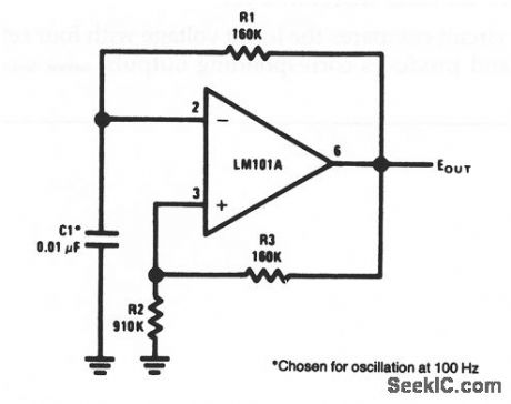
This circuit is the op-amp version of a free-running multivibrator.The square-wave output frequency is set by the value of C1. Notice that both R1 and R3 are 160 kΩ, so that output frequency is directly related to capacitance in μF, using the equation f=1/(6.28 R1C1). (View)
View full Circuit Diagram | Comments | Reading(2540)
Multiplexed_cable_driver_8_channel
Published:2009/7/24 21:34:00 Author:Jessie
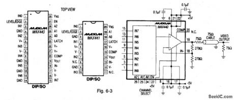
Figure 6-3 shows a multiplexer/amplifier MAX440 connected to provide 8 channels of video signal to a single cable. Unity-gain bandwidth is 160 MHz, 6-dB-gain bandwidth is 110 MHz, channel-switch time is 15 ns, slew rate is 370 V/μs, and on/off input capacitance is 4 pF. MAXIM NEW RELEASES DATA BOOK, 1993, P. 3-15. (View)
View full Circuit Diagram | Comments | Reading(635)
Multiple_aperture_window_discriminator
Published:2009/7/24 21:28:00 Author:Jessie
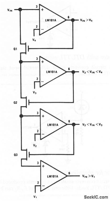
This circuit compares the input voltage with four reference voltages (V1 through V4) and produces corresponding outputs. (View)
View full Circuit Diagram | Comments | Reading(28)
Voltage_follower_with_increased_accuracy_001_μF
Published:2009/7/24 21:59:00 Author:Jessie
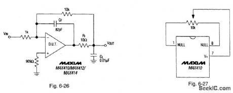
Figure 6-26 shows a voltage follower with increased accuracy (see Fig. 6-1 for pin configurations). The feedback around isolation resistor R1 increases the accuracy and the load capability. To drive capacitive loads greater than 0.01 μF, increase the value of CF. Figure 6-27 shows a null offset circuit suitable for the circuits of Figs. 6-22, 6-24, and 6-26. MAXIM NEW RELEASES DATA BOOK, 1994, P. 3-42. (View)
View full Circuit Diagram | Comments | Reading(696)
Voltage_follower_with_capacitive_load_above_100_pF
Published:2009/7/24 21:58:00 Author:Jessie
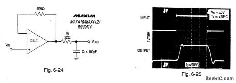
Figure 6-24 shows a voltage-follower circuit with a capacitive load above 100 pF.Figure 6-25 shows the waveforms. (see Fig. 6-1 for pin configurations). Resistor R1 isolates the load capacitance from the amplifier output to prevent oscillation.MAXIM NEW RELEASES DATA BOOK, 1994, P. 3-41. (View)
View full Circuit Diagram | Comments | Reading(734)
Voltage_follower_with_capacitive_load_100_pF
Published:2009/7/24 21:58:00 Author:Jessie
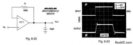
Figure 6-22 shows a basic voltage-follower circuit with a capacitive load. Figure 6-23 shows the waveforms (see Fig. 6-1 for pin configurations). This circuit is suitable for capacitive loads up to about 100 pF. MAXIM NEW RELEASES DATA BOOK, 1994 P. 3-41. (View)
View full Circuit Diagram | Comments | Reading(748)
Negative_reference__25_V
Published:2009/7/24 21:57:00 Author:Jessie
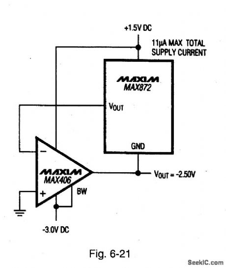
Figure 6-21 shows a MAX406 combined with a low-dropout MAX872 to form a precise -2.5-V reference that requires no external components. Typically, the MAX872 requires two external resistors. Maximum current drain is 11 μA. There is no degradation of voltage because of load regulation and no compensation is needed for load capacitance. The supplies need not have precise regulation. The positive supply can be as low as 1.1 V with the negative supply as low as 2.7 V. MAXIM NEW RELEASES DATA BOOK, 1994, P. 3-31. (View)
View full Circuit Diagram | Comments | Reading(608)
Four_channel_sample_and_holdS_H
Published:2009/7/24 21:55:00 Author:Jessie
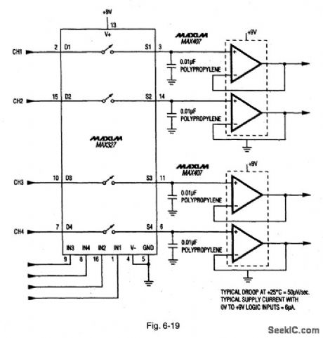
Figure 6-19 shows two MAX407s combined with a MAX327 to form a four-channel S/H circuit. See Fig. 6-18 for MAX407 pin configurations. MAXIM NEW RELEASESDATA BOOk, 1993, P. 3-30. (View)
View full Circuit Diagram | Comments | Reading(697)
Buffered_pH_probe
Published:2009/7/24 21:53:00 Author:Jessie
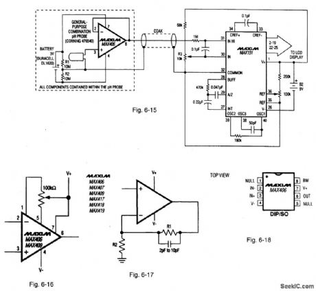
Figure 6-15 shows a MAX406 combined with a MAX131 ADC to form a buffered pH probe. This circuit eliminates expensive low-leakage cables that often connect pH probes to meters. The MAX406 and a lithium battery are included in the probe housing. A conventional low-cost cable carries the buffered pH signal to the MAX131. In most cases, the 3-V battery life exceeds the functional life of the probe.Figures 6-16, 6-17, and 6-18 show the offset-voltage adjustment, feedback compensation, and pin configurations, respectively for the MAX406. Notice that the feedback compensation (Fig. 6-17) is not required in all cases. MAXIM NEW RELEASES DATA Book, 1993, P. 3-5, 3-28, 3-29. (View)
View full Circuit Diagram | Comments | Reading(2082)
High_power_5_V_to_33_V_supply
Published:2009/7/24 22:58:00 Author:Jessie
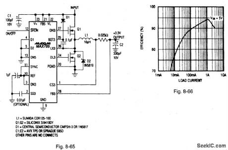
Figure 8-65 shows a MAX786 connected to provide 3.3 V from a 5-V supply. Figure 8-66 shows the efficiency curve. The circuit is suitable as a converter (possibly on a daughter card) to upgrade an existing desktop system with a new 3.3-V microprocessor. A synchronous rectifier is required. The input voltage range is 4.5 V to 6 V, with a quiescent current of 780 μA and a maximum load current capability (VIN = 4.5 V) of 3 A. MAXIM BAITERY MANAGEMENT CIRCUIT COLLECTION, 1994, P. 43.
(View)
View full Circuit Diagram | Comments | Reading(603)
SCSI_terminal_power_protection
Published:2009/7/24 22:56:00 Author:Jessie

Figure 8-64 shows how an LTC1153 can be used to protect the termination power for an SCSI (small computer serial interface) circuit. With the values shown, the dc current is limited to 1 A with a trip-delay time of 1 ms. The breaker trips if the cable or connector is accidentally shorted and will retry every second until the short circuit is removed. The termination power then returns to normal, and the interface is reconnected. The microprocessor can continuously monitor the status of the termination power (via the STATUS pin) and take further action if the fault condition persists. A gate-voltage ramp is slowed to smoothly start large capacitive loads (soft start). The circuit also includes a power-supply filter to ensure that the supply (VS) is maintained above 3.5 V until the gate is fully discharged during a short circuit. LINEAR TECHNOLOGY, APPLICATION NOTE 53, P. 16. (View)
View full Circuit Diagram | Comments | Reading(690)
Fast_half_wave_rectifier
Published:2009/7/24 22:54:00 Author:Jessie
This circuit provides rectification with 1% accuracy from dc to 100 kHz, with a slew rate of 10V/μs. Operation can be extended to full-wave rectification as shown in Fig. 10-40. (View)
View full Circuit Diagram | Comments | Reading(1612)
Electronic_circuit_breaker
Published:2009/7/24 22:54:00 Author:Jessie
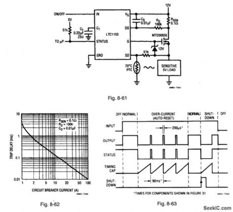
Figure 8-61 shows an LTC1153 connected for thermal shutdown. Figures 8-62 and 8-63 show the characteristics and timing diagram, respectively. The LTC1153 interrupts power to a sensitive load in the event of an overcurrent condition, and remains tripped for a period of time programmed by external capacitor CT. The switch is then automatically reset, and the load is momentarily reconnected. If the load current is still too high, the switch is shut down again. This cycle continues until the overcurrent condition is removed, thus protecting both the sensitive load and the power MOSFET. Dc trip current is set by RSEN at 1 A. The trip-delay time is set by RD and CD, and is shorter for increasing current (similar to a mechanical circuit breaker), as shown in Fig. 8-62. The circuit breaker is automatically reset (retried) every 200 ms until the overload is removed. An open-drain STATUS output warns the host microprocessor whenever the circuit is tripped. A shutdown (SD) input interfaces with a PTC thermistor to sense overtemperature conditions (over 70°C) and trip the circuit breaker. LINEAR TECHNOLOGY, APPLICATION NOTE 53, P. 15, 16.
(View)
View full Circuit Diagram | Comments | Reading(0)
Precision_clamp
Published:2009/7/24 22:53:00 Author:Jessie
In this circuit, the output is precisely clamped from going more positive than the reference voltage, preventing the op amp from saturating when D1 is reverse biased. (View)
View full Circuit Diagram | Comments | Reading(1046)
| Pages:66/126 At 206162636465666768697071727374757677787980Under 20 |
Circuit Categories
power supply circuit
Amplifier Circuit
Basic Circuit
LED and Light Circuit
Sensor Circuit
Signal Processing
Electrical Equipment Circuit
Control Circuit
Remote Control Circuit
A/D-D/A Converter Circuit
Audio Circuit
Measuring and Test Circuit
Communication Circuit
Computer-Related Circuit
555 Circuit
Automotive Circuit
Repairing Circuit