
Electrical Equipment Circuit
Index 65
ECL_to_TTL_translator_extended_range
Published:2009/7/24 9:29:00 Author:Jessie
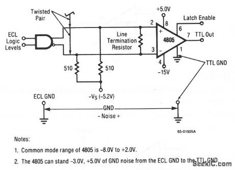
This circuit uses an RC4508 comparator as an ECL-to-TTL translator with extended common-mode range. Raytheon Linear Integrated Circuits, 1989, p. 5-13. (View)
View full Circuit Diagram | Comments | Reading(874)
DTL_TTL_driver
Published:2009/7/24 9:23:00 Author:Jessie
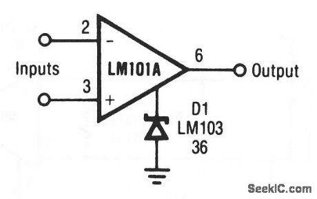
This circuit uses an LM101A as a voltage comparator to drive DTL/TTL ICs. Raytheon Linear Integrated Circuits, 1989, p. 4-247. (View)
View full Circuit Diagram | Comments | Reading(1040)
Line_synchronous_clock_multivibrator_with_high_noise_immunity
Published:2009/7/24 9:16:00 Author:Jessie
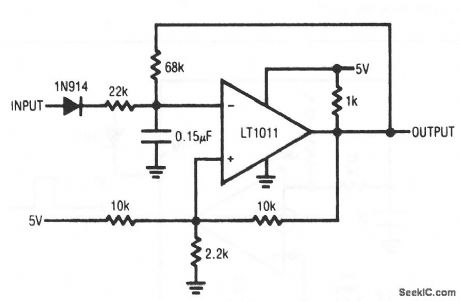
This circuit uses an LT1011 to provide a line-synchronous clock that will not lose lock under very noisy line conditions. The basic RC multivibrator is tuned to free-run near 60 Hz, but the line-derived synchronizing input forces the oscillator to lock to the line. Noise rejection is obtained from the integrator characteristics of the RC network. Linear Technology, Linear Applications Handbook, 1990, p. AN31-12. (View)
View full Circuit Diagram | Comments | Reading(698)
One_amplifier_one_shot_negative_output
Published:2009/7/24 9:16:00 Author:Jessie
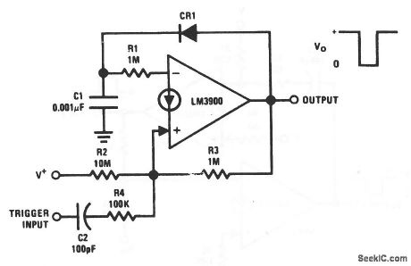
This circuit uses one LM3900 Norton amplifier to provide a negative one-shot output pulse. CR1 (a 1N914 or equivalent) permits rapid re-triggering. National Semiconductor, Linear Applications Handbook, 1991, p. 243. (View)
View full Circuit Diagram | Comments | Reading(963)
One_amplifier_one_shot_positive_output_
Published:2009/7/24 9:13:00 Author:Jessie
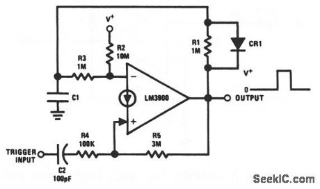
This circuit uses one LM3900 Norton amplifier to provide a positive one-shot output pulse. CR1 (a 1N914 or equivalent) permits rapid re-triggering. National Semiconductor, Linear Applications Handbook, 1991, p. 242. (View)
View full Circuit Diagram | Comments | Reading(971)
Combined_one_shot_and_comparator
Published:2009/7/24 9:12:00 Author:Jessie
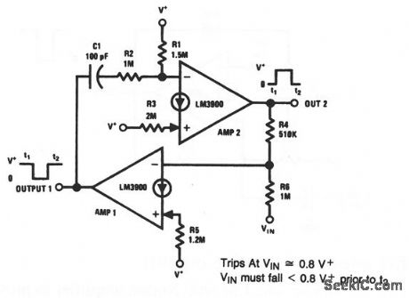
This circuit uses two LM3900 Norton amplifiers to provide a one-shot output pulse only when the input exceeds a given value (0.8 V in this case). National Semiconductor, Linear Applications Handbook, 1991, p. 242. (View)
View full Circuit Diagram | Comments | Reading(876)
Half_wave_rectifier
Published:2009/7/24 21:38:00 Author:Jessie
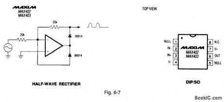
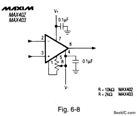
Figure 6-7 shows a MAX402/03 connected to form a half-wave rectifier. The MAX402 has a 5-V/μs slew rate and 1.4-MHz bandwidth with 75 μA for supply current. The MAX403 has a 25-V/μs slew rate and 7-MHz bandwidth, with 375 μA for supply current. Both op amps are unity-gain stable and operate from ±3 V to ±5V, or a single supply from +6 V to +10 V. Figure 6-8 shows a null circuit. MAXIM NEW RELEASES DATA BOOK, 1992, P. 3-15, 3-21. (View)
View full Circuit Diagram | Comments | Reading(0)
Neutralizing_input_capacitance_to_optimize_response_time
Published:2009/7/24 21:25:00 Author:Jessie
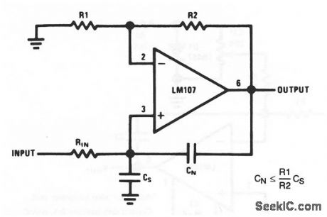
This circuit neutralizes op-amp input capacitance (which tends to restrict circuit response time). (View)
View full Circuit Diagram | Comments | Reading(795)
50_MHz_high_accuracy_analog_multiplier_with_single_ended_output
Published:2009/7/24 21:06:00 Author:Jessie
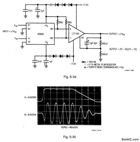
Figure 5-34 shows an analog multiplier with single-ended output. The error is within 2% over the range from dc to 50 MHz, with feedthrough below -50 dB. Figure 5-35 shows the performance when a 20-MHz sine input is multiplied by the trace A waveform, The output (trace B) is a clean instantaneous representation of the X/Y input products, with ±1 V at full scale. To trim, adjust the capacitor for minimum output square-wave peaking. LINEAR TECHNOLOGY, APPLICATION NOTE 47, P. 45. (View)
View full Circuit Diagram | Comments | Reading(759)
40_MHz_fiber_optic_receiver_with_adaptive_trigger
Published:2009/7/24 21:05:00 Author:Jessie
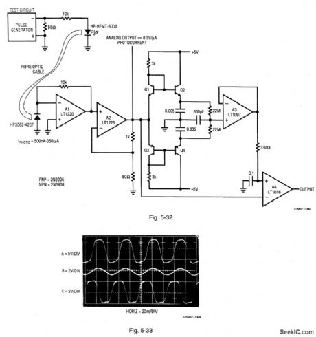
Figure 5-32 shows a circuit that will reliably condition fiber-optic inputs up to 40 MHz with input amplitudes that vary by as much as 40 dB. The digital output features an adaptive threshold trigger which accommodates varying signal intensities. An analog output is also available to monitor the detector output. Figure 5-33 shows the results of using the test circuit in Fig, 5-32. Trace A is the pulse-generator output. Trace B is the A2 output (analog output monitor). Trace C is the LT1016 output. These waveforms were recorded with a 5,ptA photocurrent at about 20 MHz. LINEAR TECHNOLOGY, APPLICATION NOTE 47, P. 44. (View)
View full Circuit Diagram | Comments | Reading(913)
Counting type peak holding circuit(CD4069,CD4081)
Published:2011/7/19 22:58:00 Author:zj | Keyword: Counting type, peak holding circuit
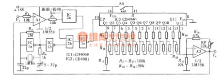
In daily life, we often need to know some physical quantities such as the maximum value, maximum velocity, maximum water level, highest temperature, maximum pressure etc. These physical quantities are usually transmitted to the measuring instrument for measuring through the associated sensor after receiving and transform and display through the instrument. And the instrument always shows the measured value at the time, this value is always changing along with the time.
(View)
View full Circuit Diagram | Comments | Reading(2553)
Quartz_stabilized_bridge_oscillator_with_common_mode_suppression
Published:2009/7/24 20:25:00 Author:Jessie
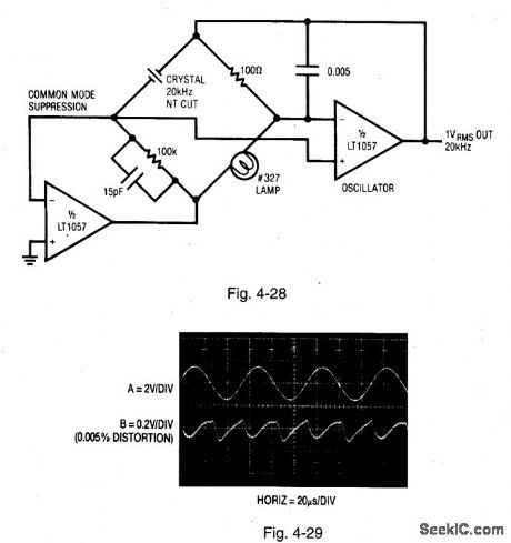
Figure 4-28 shows a bridge-oscillator circuit where the common-mode swing is suppressed by the addition of a second amplifier. This configuration forces the bridge midpoint to virtual ground by measuring the midpoint value and comparing it to ground. Because the bridge drive is complementary, the oscillator amplifier sees no common-mode swing, thus reducing distortion. Figure 4-29 shows less than 0.005% distortion(trace B)in the output(trace A)waveform.(Distortion measurements are covered In Chapter 6.) Lnvean TECHNOLOGY,APPLICATION Nom 43,P. 28. (View)
View full Circuit Diagram | Comments | Reading(684)
Fiber_optic_receiver
Published:2009/7/24 21:03:00 Author:Jessie
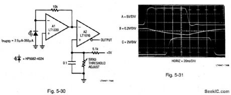
Figure 5-30 shows a simple, high-speed fiber-optic receiver. Figure 5-31 shows the waveforms. Trace A is a pulse associated with a photo input. Trace B is the A1 response, and trace C is the A2 output. A2 compares the A1 output to a dc level that is established by the threshold-adjust setting, thus producing a logic-compatible output. LINEAR TECHNOLOGY, APPLICATION Nom 47, P. 43. (View)
View full Circuit Diagram | Comments | Reading(2509)
Fast_photo_integrator
Published:2009/7/24 21:02:00 Author:Jessie
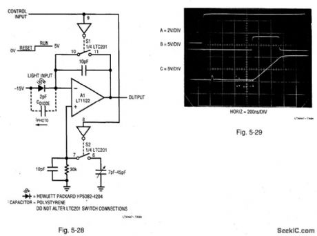
Figure 5-28 shows a photodiode-amplifier circuit that was specifically designed for situations where the total energy In a light pulse(or pulses)must be measured,The circuit is a very fast integrator, with S1 used as a reset switch, S2,switched simultaneously with S1, compensated the 51 charge-injection error. With the control input(trace A, Fig.5-29)low,and no photocurrent,51 is closed and A1 looks like a grounded follower. Under these conditions, the A1 output(trace C) remains 0 V. When the control input becomes high,A1 becomes an integrator as soon as S1 opens. At this point, the integrator is ready to receive and record a photo pulse. When light falls on the photodiode (trace B triggers a light pulse seen by the photodiode), A1 responds by integrating, and the A1 voltage (after the light event is over) is related to the total energy at the diode during the event. To adjust, cover the photodiode and set the trimmer capacitor for 0-V output from A1 (immediately after the S1/S2 switching function). LINEAR TECHNOLOGY, APPLICATION NOTE 47, P. 42. (View)
View full Circuit Diagram | Comments | Reading(2067)
Notebook_computer_porter_management
Published:2009/7/24 20:59:00 Author:Jessie
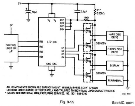
Figure 8-55 shows an LTC1156 connected to control power (and protect) for components of a notebook computer (or similar device). Each load in the circuit is activated by the microprocessor only when that component is required to process or display information. When not needed (as determined by microprocessor control), the individual systems are placed in the standby mode where quiescent current is reduced to microamp levels. The standby current of the LTC1156 is typically 16 μA with all four inputs turned off. LINEAR TECHNOLOGY, APPLICATION NorE 53, P. 10. (View)
View full Circuit Diagram | Comments | Reading(679)
High_speed_differential_line_receiver
Published:2009/7/24 20:55:00 Author:Jessie
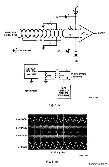
Figure 5-17 shows a simple, fast differential line receiver using an LT1194 gain-of-ten amplifier. A test circuit is also included on Fig. 5-17. Figure 5-18 shows the test results. The sine-wave oscillator drives T1 (trace A, Fig. 5-18), producing a differential-line output at the secondary. The T1 secondary is returned to ground through a broadband noise generator, flooding the inputs with common-mode noise (traces B and C are A1 inputs.) Trace D, the A1 ×10 version of the differential signal at the input, is clean with no visible noise or disturbances, in spite of the 100:1 noise-to-signal radio. LINEAR TECHNOLOGY, APPLICATIONS NOTE 47, P. 38. (View)
View full Circuit Diagram | Comments | Reading(832)
Dc_stabilization_with_differential_input_and_gain_of_10
Published:2009/7/24 20:50:00 Author:Jessie

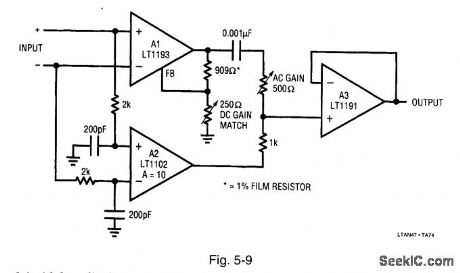
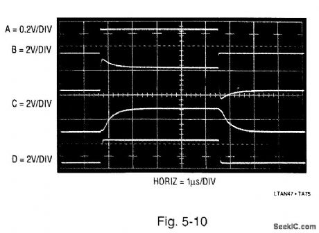
Figure 5-9 shows a way to get full differential inputs with dc-stabilized operation. Figure 5-10 shows the waveforms,Trace A is one side of the differential input applied to the circuit,trace B is the A1 output(taken at the 500-Ω pot and 0.001-μF junction),trace C is the A2 output, and trace D is the A3 output. To adjust, trim the AC GAIN pot for the squarest corners, and the DC GAIN pot for a flat top, of the output signal(trace D).Circuit gain is 10, bandwidth exceeds 35 MHz, slew rate is 450 V/pus, and dc offset is about 200 pV.LINEAR TECHNOLOGY, APPLICATION NOTE 47,P.35. (View)
View full Circuit Diagram | Comments | Reading(733)
Dc_stabilization_using_a_summing_point
Published:2009/7/24 20:43:00 Author:Jessie
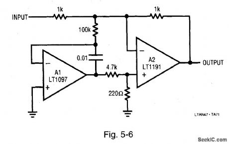
Figure 5-6 shows a circuit where the precision offset of a dc amplifier (LT1097) is combined with the bandwidth of a fast device (LT1191) to provide a dc stabilized, wideband amplifier. The LT1097 monitors the summing node (the two 1-kΩ resistors), compares the node to ground, and drives the LT1191 noninverting input. The resulting circuit is a unity-gain inverter with 35-μV offset, 1.5-V/℃ drift, 450-V/μs slew rate, and 90-MHz bandwidth. Bias current, dominated by the LT1191, is about 500 nA. LINEAR TECHNOLOGY, APPLICATION NOTE 47, P. 33. (View)
View full Circuit Diagram | Comments | Reading(881)
OTA_single_control_function_generator
Published:2009/7/24 23:54:00 Author:Jessie
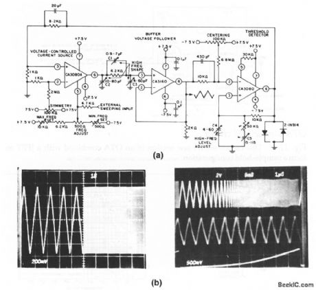
This circuit uses three sections of an OTA to form a single-control function generator that is capable of producing signals in the frequency range from 1 Hz to 1 MHz. All of the adjustments are shown on the schematic. Figure 11 -3B shows the waveforms. (View)
View full Circuit Diagram | Comments | Reading(1021)
_24_V_from_two_to_three_cells
Published:2009/7/24 23:21:00 Author:Jessie
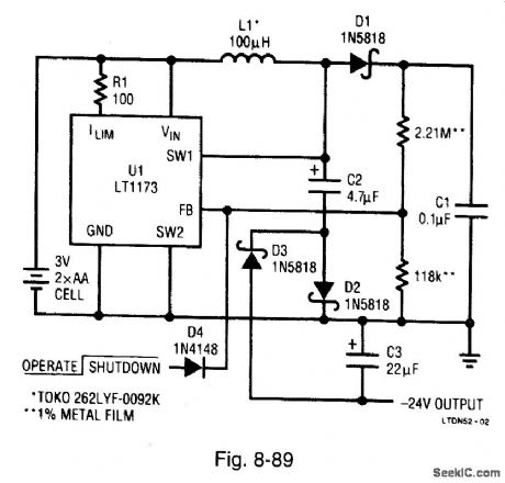
Figure 8-89 shows an LT1173 regulator connected to provide -24 V for LCD biasing using two AA cells. The 3-V input is converted to +24 V by the MOSFET switch in U1, inductor L, diode D1, and capacitor C1. The UI switch pin (SW1) then drives a charge pump composed of C2, C3, D2, and D3 to generate the -24 V.then regulation is less than 0.2% from 3.3-V to 2.0-V inputs. Load regulation, although it suffers somewhat because the -24-V output is not directly regulated, measures 2% from a 1-mA to 7-mA load. The circuit will deliver 7 mA from a 2.0-v input at 73% efficiency, and will also operate from a 5-V supply. LINEAR TECHNOLOGY, DESIGN NOTE 51, P. 1.
(View)
View full Circuit Diagram | Comments | Reading(720)
| Pages:65/126 At 206162636465666768697071727374757677787980Under 20 |
Circuit Categories
power supply circuit
Amplifier Circuit
Basic Circuit
LED and Light Circuit
Sensor Circuit
Signal Processing
Electrical Equipment Circuit
Control Circuit
Remote Control Circuit
A/D-D/A Converter Circuit
Audio Circuit
Measuring and Test Circuit
Communication Circuit
Computer-Related Circuit
555 Circuit
Automotive Circuit
Repairing Circuit