
Electrical Equipment Circuit
Index 74
TELEPHONE_OR_EXTENSION_TONE_RINGER
Published:2009/6/25 22:06:00 Author:May
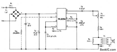
This circuit uses ML8204/ML8205 devices. With the components shown, theoutput frequency chops between 512 Hz (fH1) and 640 Hz (fH2) at a10 Hz (fL) rate. (View)
View full Circuit Diagram | Comments | Reading(1994)
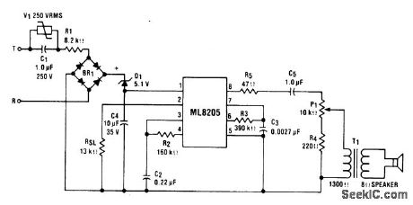
FCC_APPROVED_TELEPHONE_TONE_RINGER
Published:2009/6/25 22:03:00 Author:May
View full Circuit Diagram | Comments | Reading(1230)
TELEPHONE_TONE_RINGER
Published:2009/6/25 22:02:00 Author:May
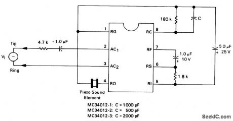
This is a complete telephone bell replacement circuit with minimum external components with on-chip diode bridge and transient protection and direct drive for piezoelectric transducers. (View)
View full Circuit Diagram | Comments | Reading(883)
TV_MODULATOR
Published:2009/6/25 21:53:00 Author:May
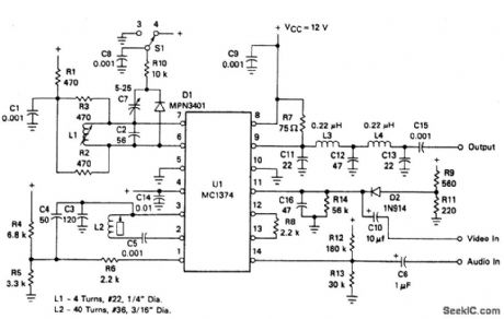
The FM oscillator/modulator is a voltage-controlled oscillator, which exhibits a nearly linear output frequency versus input voltage characteristic for a wide deviation. It provides a good FM source with a few inexpensive external parts. It has a frequency range of 1.4 to 14 MHz and can typically produce a ±25 kHz modulated 4.5 MHz signal with about 0.6% total harmonic distortion. (View)
View full Circuit Diagram | Comments | Reading(0)
TV_MODULATOR
Published:2009/6/25 21:53:00 Author:Jessie
The FM oscillator/modulator is a voltage-controlled oscillator, which exhibits a nearly linear output frequency versus input voltage characteristic for a wide deviation. It provides a good FM source with a few inexpensive external parts. It has a frequency range of 1.4 to 14 MHz and can typically produce a ±25 kHz modulated 4.5 MHz signal with about 0.6% total harmonic distortion. (View)
View full Circuit Diagram | Comments | Reading(1902)
CB_MODULATION_MONITOR
Published:2009/6/25 21:48:00 Author:Jessie
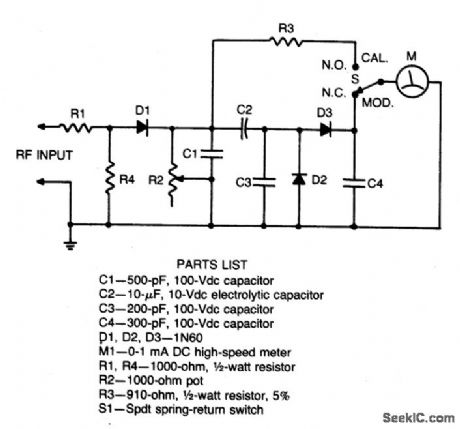
Connect this circuit to a transceiver with a coaxial T connector in the transmission line. Key the transmitter (unmodulated), set S1 to CAL, and adjust R2 for a full scale reading. Return S1 to MOD position. The meter will read % modulation with 10% accuracy. (View)
View full Circuit Diagram | Comments | Reading(1431)
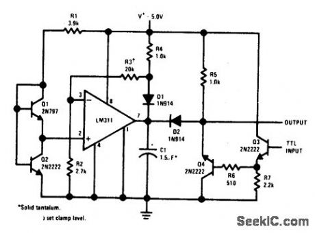
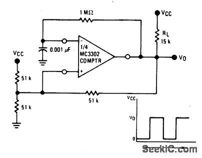
05_Hz_SQUARE_WAVE_OSCILLATOR
Published:2009/6/25 21:41:00 Author:Jessie
View full Circuit Diagram | Comments | Reading(754)
MODULATION_MONITOR
Published:2009/6/25 21:41:00 Author:Jessie
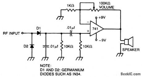
Broad-tuned recelver demodulates the RF signal picked up by a loosely coupled wire placed near the transmitting antenna. (View)
View full Circuit Diagram | Comments | Reading(1582)
WIDE_BAND_DIFFERENTIAL_MULTIPLEXER
Published:2009/6/25 21:37:00 Author:Jessie
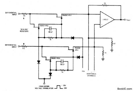
This design allows high frequency signal handling and high toggle rates simultane-ously.Toggie rates up to 1 MHz and MHz signals are possible with this circuit. (View)
View full Circuit Diagram | Comments | Reading(686)
NEGATIVE_PEAK_DETECTOR
Published:2009/6/25 21:36:00 Author:Jessie
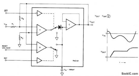
View full Circuit Diagram | Comments | Reading(1672)
PRECISION_SQUARER
Published:2009/6/25 21:36:00 Author:Jessie
View full Circuit Diagram | Comments | Reading(0)
POSITIVE_PEAK_DETECTOR
Published:2009/6/25 21:36:00 Author:Jessie
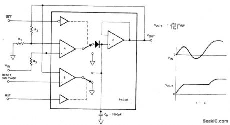
View full Circuit Diagram | Comments | Reading(3100)
MULTIPLEXER/MIXER_
Published:2009/6/25 21:35:00 Author:Jessie
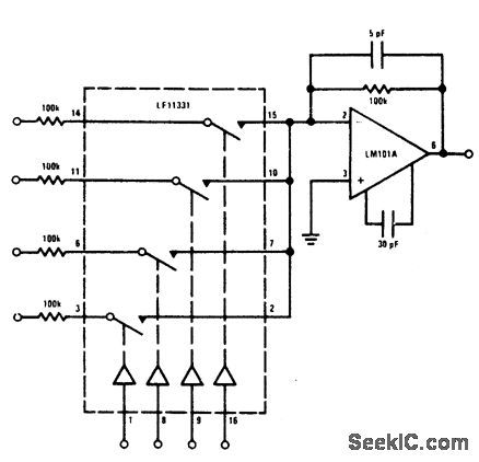
View full Circuit Diagram | Comments | Reading(690)
FREE_RUNNING_SQUARE_WAVE_OSCILLATOR
Published:2009/6/25 21:35:00 Author:Jessie
View full Circuit Diagram | Comments | Reading(665)
COMMON_SOURCE_MIXER
Published:2009/6/25 21:35:00 Author:Jessie
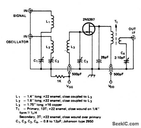
View full Circuit Diagram | Comments | Reading(648)
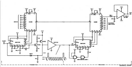
EIGHT_CHANNEL_MUX/DEMUX_SYSTEM
Published:2009/6/25 21:32:00 Author:Jessie
View full Circuit Diagram | Comments | Reading(643)
OSCILLATOR_CLOCK_GENERATOR_
Published:2009/6/25 21:31:00 Author:Jessie
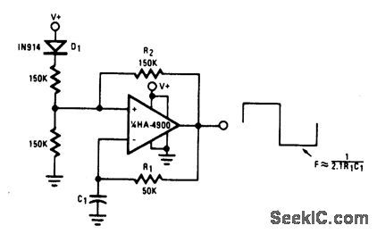
This self-starting fixed frequency oscillator circuit gives excellent frequency stability. R1 and C1 comprise the frequency determining network while R2 provides the regenerative feedback. Diode D1 enhances the stability by compensating for the difference between VOH and VSupply. In applications where a precision clock generator up to 100 kHz is required, such as in automatic test equipment, C1 may be replaced by a crystal. (View)
View full Circuit Diagram | Comments | Reading(601)
DIFFERENTIAL_MUX/DEMUX_SYSTEM
Published:2009/6/25 21:31:00 Author:Jessie
View full Circuit Diagram | Comments | Reading(662)
PRODUCT_DETECTOR
Published:2009/6/25 21:29:00 Author:Jessie
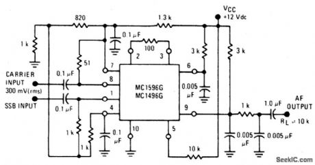
Circuit Notes
The MC1596/MC1496 makes an excellent SSB product detector. This product detec-tor has a sensitivity of 3.0 microvolts and a dynamic range of 90 dB when operating at an intermediate frequency of 9 MHz. The detector is broadband for the entire high frequency range. For operation at very low intermediate frequencies down to 50 kHz the 0.1μF capacitors on pins 7 and 8 should be increased to 1.0 μF. Also, the output filter at pin 9 can be tailored to a specific intermediate frequency and audio amplifier input impedange. The ernit-ter resistance between pins 2 and 3 may be increased or decreased to adjust circuit gain, sensitivity, and dynamic range. This circuit may also be used as an AM detector by intro-ducing carrier signal at the carrier input and an AM signal at the SSB input. The carrier signal may be derived from the intermediate fre-quency signal or generated cally. The carrier signal may be introduced with or without mod-ulation, provided its level is sufficiently high to saturate the upper quad differential amplifier. If the carrier signal is modulated, a 300 mV (rms) input level is recommended. (View)
View full Circuit Diagram | Comments | Reading(5)
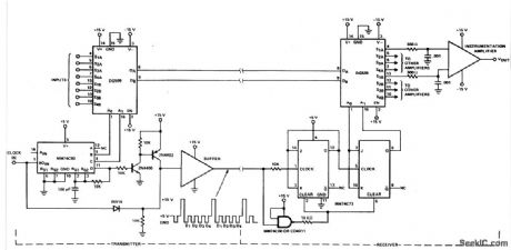
DIGITAL_TRANSMISSION_ISOLATOR
Published:2009/6/25 21:29:00 Author:Jessie
View full Circuit Diagram | Comments | Reading(1546)
| Pages:74/126 At 206162636465666768697071727374757677787980Under 20 |
Circuit Categories
power supply circuit
Amplifier Circuit
Basic Circuit
LED and Light Circuit
Sensor Circuit
Signal Processing
Electrical Equipment Circuit
Control Circuit
Remote Control Circuit
A/D-D/A Converter Circuit
Audio Circuit
Measuring and Test Circuit
Communication Circuit
Computer-Related Circuit
555 Circuit
Automotive Circuit
Repairing Circuit