
Index 192
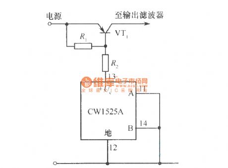
CWl525A single-ended common circuit
Published:2011/7/12 19:49:00 Author:TaoXi | Keyword: single-ended, common circuit
View full Circuit Diagram | Comments | Reading(588)
4W backup type switching power supply circuit
Published:2011/7/12 20:04:00 Author:TaoXi | Keyword: 4W, backup type, switching, power supply
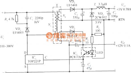
The +5V and +12V dual-channel output 4W backup type switching power supply circuit which is composed of the TOP221P is as shown in the figure. This circuit uses one piece of TOP221P(ICl) and one piece of optocoupler PC817A (IC2). The circuit can continue to supply power if the main power is failure, so it can ensure that the data of the CPU and real time clock chip internal RAM will not loss. The input port is connected with the DC voltage Ui. The value of Vi is decided by the change range of the AC input voltage u (such as 85~245V). T is the high frequency transformer, N1 is the primary coil, N2 is the subprime coil, N3 is the feedback coil.
(View)
View full Circuit Diagram | Comments | Reading(1977)
J8O-1A57-the communication single chip microcomputer integrated circuit
Published:2011/7/13 10:46:00 Author:Borg | Keyword: communication single chip, microcomputer
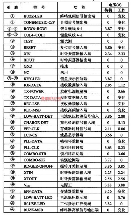
1.function featuresJ80-1A57 contains the wireless emitting and receiving control circuit, key switch encoding/decoding circuit, charge detection circuit, battery low-voltage circuit, PLL signal process circuit, keypad indicator control circuit, field strength detection circuit, buzzer drive control circuit, 2 lines of clock oscillating circuits, ringing switch control circuit and other indicator drive control circuit, etc.2.pin functions and dataJ80-1A57 is in 44-pin package, whose pin functions and data are listed in table 1-1.
(View)
View full Circuit Diagram | Comments | Reading(618)
+5V, 1.6A precision switching power supply circuit
Published:2011/7/12 21:19:00 Author:TaoXi | Keyword: +5V, 1.6A, precision, switching, power supply
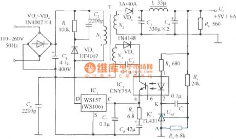
The +5V, 1.6A precision switching power supply circuit is as shown in the figure. This circuit increases the photoelectric coupler (CNY75A) and the adjustable precision parallel regulator (TIA31). R3 is the current limiting resistor, R4 and R5 are the sampling resistor. When the Vo changes, the sampling resistor will compare with the 2.5V reference voltage of the TL431, so the electric potential of the K port changes to change the LED's operating current and the luminous intensity of the CNY75, then it adjusts the control port current of WSl57 through the optocoupler, so you can fine-tune the duty cycle to realize the purpose of precision voltage. The CNY75A has also played the electrical isolation effect.
(View)
View full Circuit Diagram | Comments | Reading(5334)
+12V, 0.5A single chip switching power supply circuit
Published:2011/7/12 21:27:00 Author:TaoXi | Keyword: +12V, 0.5A, single chip, switching, power supply
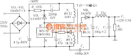
The +12V, 0.5A single chip switching power supply circuit is as shown in the figure. The output power is 6W. When the input AC voltage is in the range of 110~260V, the voltage relative regulation Sv≤1%, when the load current changes greatly, the load relative regulation SI=5%~7%. In order to simplify the circuit, we use the basic feedback mode.
After you connect the power, the 220V AC is bridge type rectified and filted by C1 firstly to get the +300V DC high voltage, then it supplies the operating voltage to WS157 through the primary coil N1 of the high frequency transformer.
(View)
View full Circuit Diagram | Comments | Reading(4187)
15V/3.5A 52W switching power supply circuit
Published:2011/7/12 21:49:00 Author:TaoXi | Keyword: 15V/3.5A, 52W, switching, power supply circuit
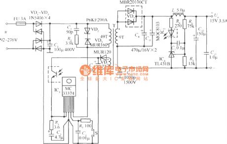
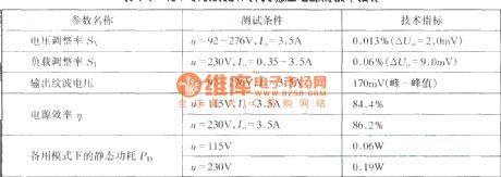
The 15V/3.5A 52W switching power supply circuit which is composed of the MC33374T/TV is as shown in the figure. The permitted range of the AC input voltage u is 92~276V. The rectifier bridges VD1~VD4 use four 1N5406 type 3A/600V siliconrectifier tube. The primary protection circuit is composed of the RC absorbing circuit (R2, C2) and the clamping circuit (VDz, VD5), it can effectively inhibit the peak voltage which is produced the leakage inductance of the high frequency transformer to protect the MC33374 internal power switching tube away from the damage. The VDz uses the P6KE200A type transient voltage suppression diode (TVS), the reverse breakdown voltage UB=200V. The VD5 uses the MURl60 type ultrafast recovery diode (SRD).
(View)
View full Circuit Diagram | Comments | Reading(1566)
Homemade maintenance and charging dual-function power supply circuit
Published:2011/7/13 4:53:00 Author:TaoXi | Keyword: Homemade, maintenance, charging, dual-function, power supply

Operating principle of the low voltage output: the 32V voltage of the transformer subprime stage is rectified by VD1-VD4 and filted by the C1, so we get the 45V DC voltage, this DC voltage changes into the stable output voltage through the integrated three-port voltage stabilizer LM338K, you can get the 1.25V-37V stable DC voltage from the output port by adjusting the potentiometer RP1. In the figure, the LED1 is the indicator light of the regulated power supply, R1 is the current-limiting resistance of LED1, C2 can be used to filter the high-frequency harmonic components of the power supply and eliminate the parasitic oscillation. The VD5 and VD6 can be used to prevent the input and output short circuits to protect the LM338K.
(View)
View full Circuit Diagram | Comments | Reading(944)
Storage battery automatic charger circuit (1)
Published:2011/7/13 19:17:00 Author:TaoXi | Keyword: Storage battery, automatic charger
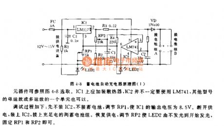
The circuit is as shown in figure 4-8. FU is the short circuit protection tube, LED1 is the power supply instruction, you can change the output voltage of IC1 by changing IC1, the center port of RP2 supplies the reference voltage to the positive phase input port of the voltage comparator IC2, R3 is the charge current sampling resistance, VD can be used to prevent the battery discharging, LED2 is the charging state instruction, C1 and C2 can be used to prevent the pulse interference.
The control principle of the stop-charging is: the charging current decreases with the charging process, and the voltage drop of R3 decreases too. If it is lower than the set value of RP2, the electrical level of pin-2 is lower than the electrical level of pin-3, pin-6 has the low electrical level, VD is in the reverse biasing state, the charging current is 0.
(View)
View full Circuit Diagram | Comments | Reading(871)
Storage battery automatic charger circuit (2)
Published:2011/7/13 19:28:00 Author:TaoXi | Keyword: Storage battery, automatic charger
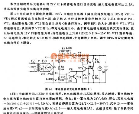
The principle diagram of the storage battery automatic charger circuit is as shown in the figure 4-9. The 220V city electricity is reduced by the transformer T to get the secondary voltage U2, and this secondary voltage U2 is bridge-type rectified to output the DC pulse voltage, the DC pulse voltage gets through the relay normally closed contact points K1-2,the R4, the ammeter PA, the VT1 and the battery GB, the VT2 to charge the GB. You can adjust the base potentials of VT1 and VT2 by adjusting RP1, so that you can adjust the Icb charging current of VT2. For example, when the battery voltage of the 12V storage battery increases to (12/2)X2.5=15V, VT3 conducts, K1 closes, the normally closed contact points K1-2 cut off to cut off the charging circuit, the charger will stop charging.
(View)
View full Circuit Diagram | Comments | Reading(779)
Switching power supply thick film integrated circuit diagram
Published:2011/6/14 7:23:00 Author:Sophia | Keyword: Switching power supply, thick film integrated circuit
STR一D6601 produced by Sanken company is Switching power supply thick film integrated circuit. The improved products of STR一D6601 is widely used in Hitach and Furistock 64cm color TV and VCD, DVD player.
1. The function and characteristics of STR一D6601STR一D6601 integrated circuit contains distributary, driving circuit and high-power switching tube. The peak power output reaches 120w.
2. The function and data of the pin
STR一D6601 integrated circuit adopts single-row pin capsulation, the function and data of its integrated circuit is shown by the chart 1.
note: the output power of STR-D6601 is larger than that of FbSTR-6601, so FbSTR-6601 can replace STR-6601,never the other way around
(View)
View full Circuit Diagram | Comments | Reading(826)
STR D5095A Switching power supply thick film integrated circuit diagram
Published:2011/6/14 7:23:00 Author:Sophia | Keyword: STR D5095A Switching power supply, thick film integrated circuit
STR一D5095A produced by Sanken company is low power consumption and high-power Switching power supply thick film integrated circuit and is widely used in Hitach sz large screen movement of color TV.
1. The function and characteristicsSTR一D5095A integrated circuit contains sampling, erro amplification, driving circuit, high-power switchiing tube and some other miscellaneous function.
2. The function and data of the pinthe function and data of its integrated circuit is shown by the chart 1. the resistance of the circuit:red pen measurement means that the black probe connects 1 pin. the red probe connect the value of the measured pin;black probe mesurement means that red probe connects 1 pin. Black probe connects the resistance value of the measured pin. (View)
View full Circuit Diagram | Comments | Reading(3619)
Switch Power Supply Circuit of Operational Amplifier A741
Published:2011/6/15 10:40:00 Author:Michel | Keyword: Operational Amplifier, Switch Power Supply, Circuit
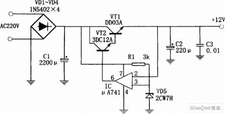
The picture shows a novel design of switch power.The power adopts operational amplifier A741 as comparing control elements, two transistor as adjustable components and the circuit work in switch state.When the output voltage is 2mV lower than benchmark low voltage,in other words,μA741 ② feet is 2mV lower than ③ feet(Because μA741 response sensitivity is 2mV),μAT41 ⑥ feet outputs high PWL,control VT1 and VT2 conduct and load with large current and relevant filter capacitors,C2 and C3 supply power which makes output voltage increases to 12V,that's to say,both μA741 ② and ③ feets' potential are equal.The⑥ feet outputs low voltage (2 V), VT1, VT2 close and it suspends supply electric power.As the time goes by, the output voltage drops grdually and repeats the aboved process,the power keeps in swtich state and the output voltage is 12V all the time. (View)
View full Circuit Diagram | Comments | Reading(1413)
Micro Controller MC9S08AW32 and HT1621 Interface Circuit
Published:2011/6/15 8:16:00 Author:Michel | Keyword: Micro Controller, Interface Circuit

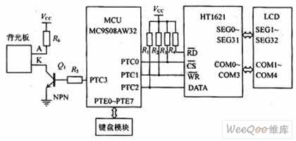
Liquid crystal display system hardware interface circuit mainly contains micro controller,MC9S08AW32, liquid crystal display module LCD, backlight,liquid crystal drive chip HT1621,key module and resistance and capacitance components etc. and it is showed as the figure 1.
In the figure 1, PTC0 ~ PTC2 port of micro controller MC9S08AW32 are connected to liquid crystal drive chip HT1621's chip selecting signal port (CS), write signal control port (WR) and data signals port (DATA)respectively and they connect pull-up resistors to high PWL respectively. Read signal control port (RD) only needs to connect to high PWL via pull-up resistors because there is no necessary to use HT1621's Read operation.The MC9S08AW32 PTE0 ~ PTE7 port connects key module, PTC3 port connects NPN transistor, which is to control back panels. (View)
View full Circuit Diagram | Comments | Reading(3187)
Relaxation Oscillation Circuit of Unijunction Transistor
Published:2011/6/14 13:12:00 Author:Michel | Keyword: Unijunction Transistor, Relaxation Oscillation Circuit
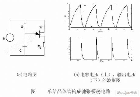
The relaxion oscillating circuit which is composed of uijunction transistor is showed as the picture (a).The initial voltage of capacitor is set to 0.The power supply charges the capacitancevia the resistance R when the power is switched UA of uijunction transistor depends on power voltage E(Ubb) and devices' current-voltage characteristic and peaks and valleys point are also determined by this.Capacitor voltage rises in accordance with the index.Emitter current is small before emitter voltage reaches peak and two ends voltage can be ignored becuase the current that passes through R1 is very small.The uijunction transistor enters negative resistance area and then the diode current flows when the voltgae reaches the peak and UC is equal to UP. (View)
View full Circuit Diagram | Comments | Reading(762)
17W PC Standby Power Supply Circuit of 5V and 3.3 V Output
Published:2011/6/14 13:11:00 Author:Michel | Keyword: 5V , 3.3 V, Standby Power Supply
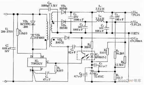
The picture 3 shows the PC standby circuit which provides both 5V,2A and 3V,2A 's main output.This power supply adds 15V,30mA's auxiliary output with lowest cost.This circuit uses a TOP232Y type singlechip power supply and its total output supply is 17.05W.DC input voltage range is 200~375V. 110V AC 220 / fixed input voltage can be chosen as long as it isconnected to commuting filter and it is unnecessary to add voltage multiplier to commutate 110V AC.This design fully takes TOP232's advantages such as soft start, voltage protection, strictly limited flow characteristics and high switching frequency and its advantages make the high-frequency transformer choose EE19 type chip. (View)
View full Circuit Diagram | Comments | Reading(3321)
Step Voltage Generating Circuit of Output Fifth Voltage
Published:2011/6/14 13:18:00 Author:Michel | Keyword: Fifth Voltage, Step Voltage, Generating Circuit
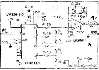
Circuit's Functions
Ladder is a waveform that voltage shows ladder shape change with the time increases.In other words,it's a kind of bad slope linear waveform caused by digital circuit.In this circuit,at most 15 steps voltage can be output.The average time of per level is determined by external input clock and level differences of output voltage are equal.This cuircuit can be used if you want to gradually improve the response of the voltage.
Circuit's Work Principle
C1 is four binary counter and it constitutes 4 D - A converter when R - 2R trapezoidal resistor network are added to its output terminal.
(View)
View full Circuit Diagram | Comments | Reading(665)
Numerical Control D. C. Regulated Power Supply Four
Published:2011/6/14 12:55:00 Author:Michel | Keyword: Numerical Control, D. C., Regulated Power Supply, Four
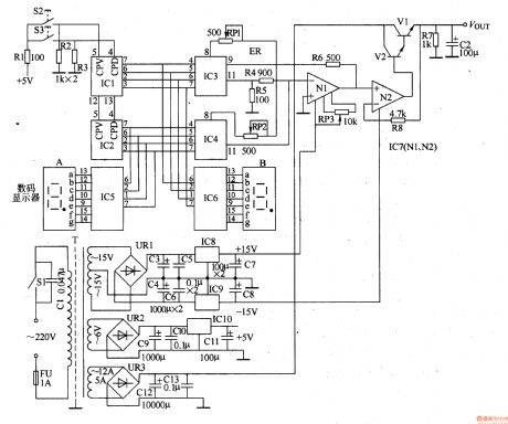
The numerical control D. C. regulated power supply circuit introduced in the example adopts LED to indicate output voltage's magnitude with features of visual display,convenient operation,high-precision voltage regulation.Its output voltage range is 0-9.9V and output current is 5A.
Circuit's Work principle
The numerical control D. C. regulated power supply circuit is composed of power regulation voltage circuit,operation and control circuit,display driver circuit,D/A converter circuit and regulated output circuit and it is showed as the picture 5-23.The power regulation voltage consists of mains switch,S,fuse,FU,mains transformer,T,rectifier bridge,UR1-UR3,capacitor,C1,C3-C13 and voltage regulation IC,IC8-IC10. (View)
View full Circuit Diagram | Comments | Reading(855)
Numerical Control D. C. Regulated Power Supply Fourteen
Published:2011/6/14 12:54:00 Author:Michel | Keyword: Numerical Control, D. C., Regulated Power Supply, Fourteen
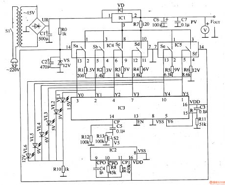
The numerical control D. C. power-supply circuits-fixed introduced in the example uses single button control means and its magnitude of output voltage are divided into six grades,namely,1.5 V,3V,5V,6V,9V and 12V.Its output power is 20W.Its femature is that open it after cutting off utility power and the output voltage is the lowest voltage,1.5V
Work's Principle of the Circuit
The numerical control D. C. power-supply circuits-fixed is composed of input constant voltage circuit,impulsator,control output or indication circuit and it is showed as the picture5-33.The input constant voltage circuit consists of ,switch,S1,mains transformer,T,rectifier bridge,UR,filter capacitor,C1,C2,current-limiting resistor,RO and voltage regulator diode,VS. (View)
View full Circuit Diagram | Comments | Reading(938)
DC boost circuit
Published:2011/7/10 19:36:00 Author:John | Keyword: DC boost
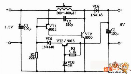
DC step-up is to upgrade the lower DC battery voltage to a required voltage. The basic work process is shown in the following: firstly the low-voltage pulse is throughhigh-frequency oscillation; then a predetermined voltage value is stepped-up by a pulse transformer; afterwards, high-voltage direct current is obtained by pulse rectifier. Thus, DC boost circuit is classified into DC / DC circuits.
In the portable battery-powered devices, the high voltage required in the circuit is usually obtained by DC boost circuits. These devices include cell phones, pagers, other wireless communications equipment, camera flash, portable video display device and power equipment such as electric shock and so forth.
(View)
View full Circuit Diagram | Comments | Reading(1649)
UC3844 60W switching power supply circuit diagram
Published:2011/6/18 9:55:00 Author:Nancy | Keyword: 60W, switching power supply
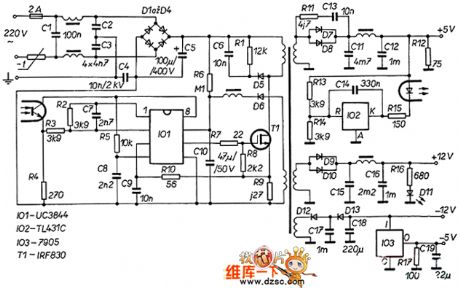
View full Circuit Diagram | Comments | Reading(8634)
| Pages:192/291 At 20181182183184185186187188189190191192193194195196197198199200Under 20 |
Circuit Categories
power supply circuit
Amplifier Circuit
Basic Circuit
LED and Light Circuit
Sensor Circuit
Signal Processing
Electrical Equipment Circuit
Control Circuit
Remote Control Circuit
A/D-D/A Converter Circuit
Audio Circuit
Measuring and Test Circuit
Communication Circuit
Computer-Related Circuit
555 Circuit
Automotive Circuit
Repairing Circuit