
Index 182
The dual-channel long-line transmission circuit
Published:2011/7/20 22:31:00 Author:Borg | Keyword: dual-channel, long-line transmission
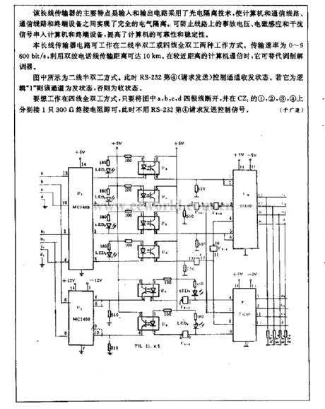
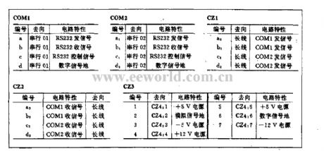
The main feature of the long-line transmission is that the input and output circuits are adopted with the photoelectric separation technology, which fulfills the full electric separation between the computer and communication line, communication line and the terminal equipment. So the accident voltage, electromagnet inductance and disturbance signal are prevent from running into the computer and the terminal equipment, and the reliability and stability of the computer are improved.
(View)
View full Circuit Diagram | Comments | Reading(642)
The KJ004 SCR phase drifting trigger circuit
Published:2011/7/20 22:51:00 Author:Borg | Keyword: phase drifting, trigger circuit
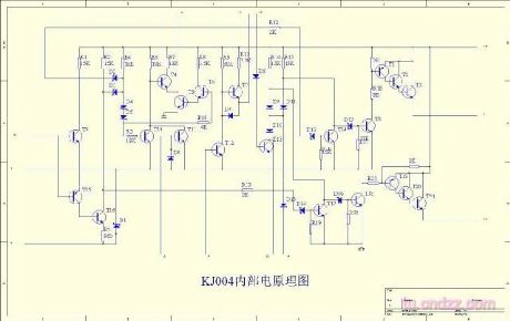
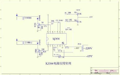
The KJ004 SCR phase drifting trigger circuit is suitable for the single phase, 3-phase bridge power supply devices as the dual-channel pulse phase drifting trigger of SCR. KJ004 outputs two lines of drifting pulses which differ 180⁰, so they can easily compose the full-control bridge trigger line. The circuit characterizes large load, good transposition, good balance of the forward/backward pulse, wide transposition range, low requirement on synchronous voltage, output terminal with pulse modulation and so on.
(View)
View full Circuit Diagram | Comments | Reading(2451)
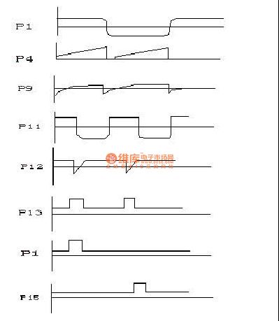
The dual-channel infrared sound volume remote control circuit
Published:2011/7/20 22:40:00 Author:Borg | Keyword: sound volume, remote control
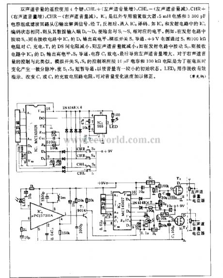
The dual-channel sound volume remote control uses 4 keys: CHL+(the left sound channel volume increases), CHL-(the left sound channel volume decreases), CHR+(the right sound channel volume increases), CHR-(the right sound channel volume decreases). IC1 is the preamplifier of infrared, the 5mH inductor and 3300pF capacitor compose the filter circuit which outputs the modulation signal from ①, the signal is sent to IC2 for decoding after its phase is reversed by T1.
(View)
View full Circuit Diagram | Comments | Reading(607)
The DC booster circuit fitted in multimeters
Published:2011/7/20 22:23:00 Author:Borg | Keyword: DC booster, multimeters
The multimeter is a necessary tool for the electrician and electric technique worker, whose high impedance gear often uses a laminated cell of 9V, 15A or 22.5A. The cell is not only costly, but also short-lived, so it's not economic to change it often. Here is to introduce some small DC booster circuits which are fitted for the multimeter. These circuits are simple and they have few elements, after conversion, they can be directly installed in the laminated cell position to replace the cell. (View)
View full Circuit Diagram | Comments | Reading(616)
The thyristor voltage regulation circuit with the output power of 1-4KvA
Published:2011/7/20 22:15:00 Author:Borg | Keyword: voltage regulation circuit, output power
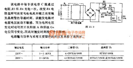
The capacitor C in the circuit is charged by R3 and R4 every half wave. The charge current changes if the resistance of R4 is changed, and the conducting time of the trigger thyristor is changed. The trigger circuit is not sensitive to the power supply voltage deviation. As the LEV of the positive pole A and negative pole Ga of the SCR switch changes when the grid voltage changes, so it doesn't affect the trigger time.
(View)
View full Circuit Diagram | Comments | Reading(686)
The data general line test circuit
Published:2011/7/20 22:07:00 Author:Borg | Keyword: general line
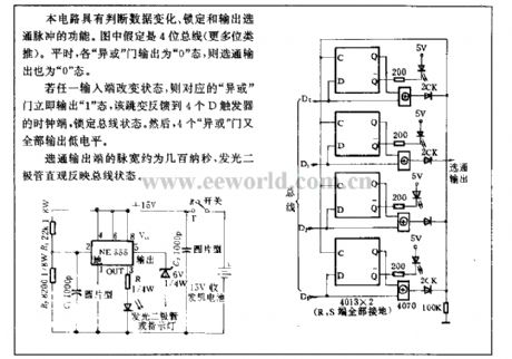
The circuit can judge the data change, lock and output the strobe pulse. In the figure, we assume it is the 4-bit general line(more bit analogy). Usually, each OR gate outputs 0 , and the strobe output is also 0 . If each input terminal changes its state, the corresponding OR gate will output 1 quickly, the jump is fed back to 4 clock terminals of D trigger, which locates the general line. Then, all of the 4 OR gates output the low LEV.
(View)
View full Circuit Diagram | Comments | Reading(616)
the digital separation circuit
Published:2011/7/20 21:58:00 Author:Borg | Keyword: digital separation circuit
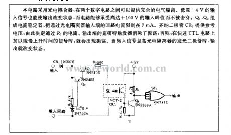
The circuit is fixed with a photoelectric coupler, which can fully separate the electricity between 2 digital circuits. The low voltage input signal of +4V can also change the output state, and the circuit can afford the peak value of +100V without being broken down. Q1 and Q2 compose the current stabilizer, which limits the current at 7mA through the input terminal of the photoelectric separator. The Zener diode CR2 provides with the Vref which decides the current of R2.
(View)
View full Circuit Diagram | Comments | Reading(574)
the digital clock circuit
Published:2011/7/20 21:51:00 Author:Borg | Keyword: digital clock
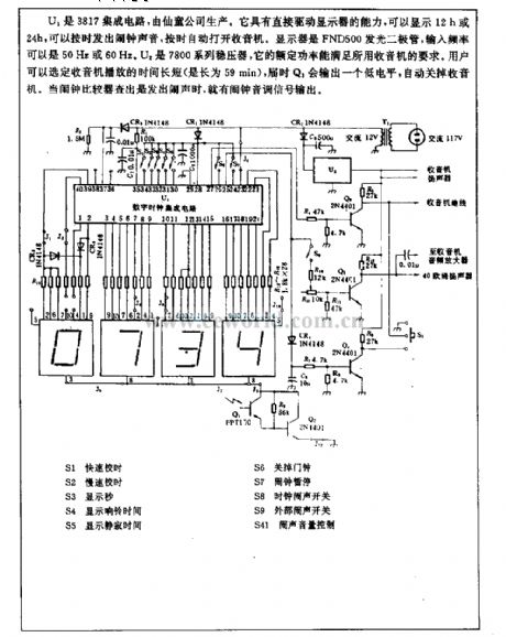
U1 is a 3817 integrated circuit, which is produced by Fairchild Corp. It can directly drive the display, and it can display for 12h or 24h, It can generate the clock sound and turn on the radios on time. The display is a FND500 LED, the input frequency can be 50Hz or 60hz. U2 is a 7800 voltage stabilizer whose regulated power can meet all radio users' need. The users can choose the radio working time length(the max time is 59min).
(View)
View full Circuit Diagram | Comments | Reading(2146)
the digital pulse width test circuit
Published:2011/7/20 21:44:00 Author:Borg | Keyword: pulse width, test circuit
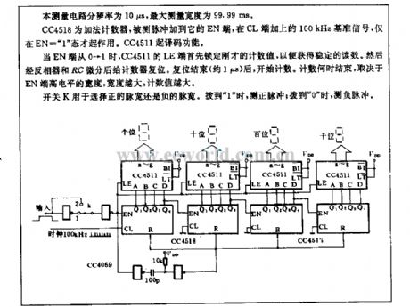
The definition of the test circuit is 10μs, the Max test width is 99.99ms. CC4518 is the adding counter, the pulsed under test is added on its EN terminal, the 100kHz reference signal is added on the CL terminal, only when EN=1 does the counter work. CC4511 works as the decoder. When EN changes from 0 to 1, the LE of CC4511 locates the counting number firstly, so the stable reading can be acquired. Then the counter is reset after it is differentiated by the phase reverser and RC.
(View)
View full Circuit Diagram | Comments | Reading(613)
the digital watch circuit
Published:2011/7/20 21:34:00 Author:Borg | Keyword: digital watch
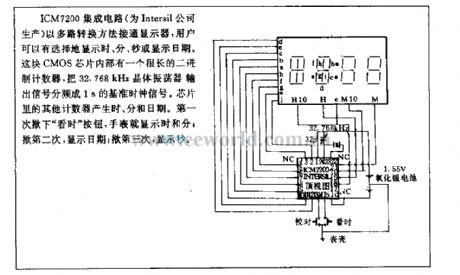
The ICM7200 integrated circuit (produced by Intersil Corp.) connects with the screen in multi-channel method, the user can selectively display the H, M, S or the date. This CMOS chip contains a long binary counter, which splits the 32.768KHz crystal oscillator input signal into the 1s reference clock signal. The other counters generate the H, M and date. When the key of see the time is pressed for the first time, the watch will display the hour and minute; when it is pressed for the second time, the watch will display the date and the second will be displayed for the third time.
(View)
View full Circuit Diagram | Comments | Reading(1602)
The pilotless car circuit of double motors
Published:2011/7/20 21:24:00 Author:Borg | Keyword: pilotless car
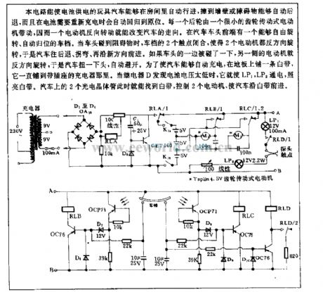
The circuit can make the toy car with battery power supply move automatically, and the toy car can back off automatically when it touches the wall or the obstacle, it will reset automatically when the cell needs to be recharged. Each rear wheel is driven by a wheel gear motor, so just the reversed running of one motor can control the moving direction of the car. At the head of the car, there is a car gear which can freely rotate and reset automatically.
(View)
View full Circuit Diagram | Comments | Reading(662)
The solar auto tracking control circuit
Published:2011/7/20 20:40:00 Author:Borg | Keyword: solar, auto tracking, control circuit
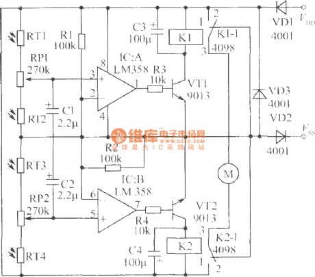
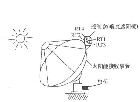
See as the figure, the dual op-amp LM358 composes 2 voltage comparator with R1 and R2, the Vref is 1/2 of VDD(+12V). The LDR of RT1 and RT2 with RP1, RT3 and RT4 with RP2 compose the light dependent sensing circuit respectively, one special thing of the circuit is that it can automatically self-compensate according to the light. See as the figure, RT1 and RT3 are installed at one side of longitudinal sunshading board, while RT4 and RT2 at the other side.
(View)
View full Circuit Diagram | Comments | Reading(3594)
The general counter circuit
Published:2011/7/20 21:11:00 Author:Borg | Keyword: general counter
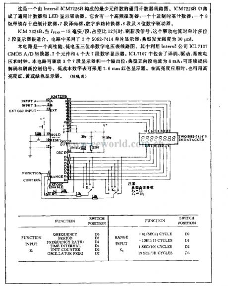
This is a general counter circuit with the least elements, which consists of Intersil ICM7226B. ICM7226B integrates the general counter and the LED display driver, it contains a HF oscillator, a decimal time-based counter, an octal lock decimal counter, 7-stage decoder, digital multi-channel converter, 8-stage and 8-bit digit driver. When Ipeak=15mA/S, duty cycle is 12%, ICM7226B will refresh the stage signal.
(View)
View full Circuit Diagram | Comments | Reading(654)
The auto control energy saving lamp circuit composed of solar battery
Published:2011/7/20 20:48:00 Author:Borg | Keyword: energy saving lamp, solar battery
See as the figure, the solar auto control energy saving lamp circuit consists of the solar cell charger, light control switch, timing switch and reversing circuit. To light the energy-saveing lamp, both the light control and timing switches are connected. At daytime, the sunlight is shed on the solar cell board, which converts the light power into electricity and charges the storage cell with the help of the diode VD1. (View)
View full Circuit Diagram | Comments | Reading(1601)
Single-supply operation of the operational amplifier input protection circuit
Published:2011/7/16 9:41:00 Author:Sophia | Keyword: Single-supply operation, the operational amplifier input protection
The diagram a, b is a single-supply op amp input protection circuit, the diode VD2 is connected between the op amp input and the ground. In Figure (a) and Figure (b) the resistance R is 1kΩ, but in low-noise circuit, which the circuit performance is influenced by the thermal noise of the resistance itself, the smaller the resistance R of 100Ω resistance, the smaller the effect of Thermal noise. (View)
View full Circuit Diagram | Comments | Reading(1548)
High precision ±18V bipolar regulated power supply circuit diagram
Published:2011/7/18 5:34:00 Author:nelly | Keyword: bipolar regulated power supply, ±18V regulated power supply
View full Circuit Diagram | Comments | Reading(2026)
the CATV 60V switch power supply circuit
Published:2011/7/20 0:01:00 Author:Borg | Keyword: switch power supply
To reduce the wave of the output, the input terminal of the circuit is using full-wave double rectifier, the output wave is reduced by increasing the AC voltage. The practice proves it can get good results. With ordinary methods, the 60V AC is rectified, if we want to get the same low output wave, at least 5 470u/160v capacitors can filter the wave. The parameters are as follows: input AC voltage is 35-70V, output DC voltage is 24V, output DC current is 0.65A, output wave (full load) is ≤15mV(Vp-p). (View)
View full Circuit Diagram | Comments | Reading(2465)
555 positive voltage converting to 5v power supply circuit
Published:2011/7/24 4:06:00 Author:Lucas | Keyword: 555 positive voltage , 5v power supply
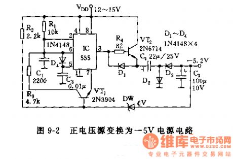
The 555 and R1, C1, VT1 and other components in Figure 9-2 form a multivibrator with the oscillation frequency being determined by R1, C1, R3 . C1 charges through R1, when the the potential of pin 6 charges to above 2/3 VDD of the threshold level, the 555 resets, pin 3 is at low level. DW is a Zener diode, when the negative output voltage is prompted to turn on D5, VT1 remains cut-off state. When the load current makes C1 discharge to a certain extent, D5 is deadline, and VT1 is turned on, then C1 begins to charge. The oscillation frequency of 555 changes with a certain load. Power load adjusted rate is about 1.5%.
(View)
View full Circuit Diagram | Comments | Reading(842)
The heavy current and high efficiency switch constant voltage power supply circuit formed by LAS6351
Published:2011/7/20 23:40:00 Author:leo | Keyword: Heavy current, high efficiency
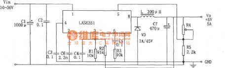
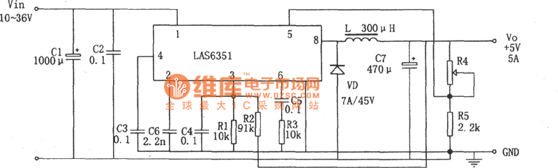 As the picture shows, it is a heavy current and high power switch constant voltage power supply circuit formed by LAS6351. LAS6351 is a kind of switch integrated AVR which has heavy current and adjustable impulse width. It can output 2.5 V to 5 V voltage under 3 A to 8 A constant load current. It has soft boot and over load, over voltage as well as over current protecting circuits. Its efficiency can reach 90%. Because of the 200kHz efficiency, the cost of outer filter is lowered down. (View)
View full Circuit Diagram | Comments | Reading(788)
Simple multi-function charger circuit
Published:2011/7/15 4:09:00 Author:TaoXi | Keyword: Simple, multi-function, charger
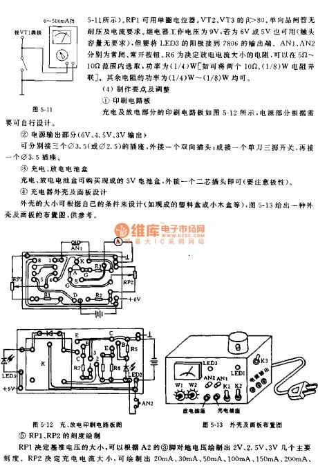
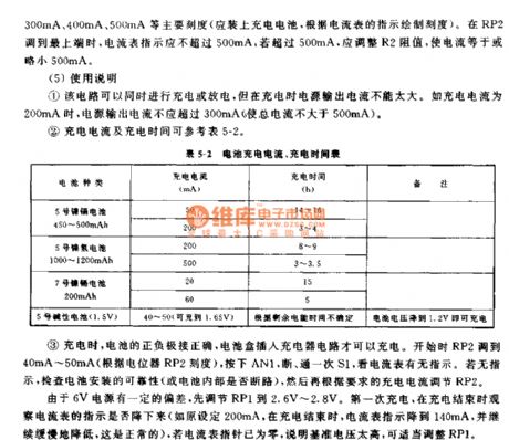
Operating principle:
This circuit has four parts: the charging circuit, the discharging circuit, the power supply circuit and the lighting circuit, as shown in figure 5-8. The power supply circuit part can output the 6V, 4.5V, 3V voltage, the output current is 500mA, it can be used to provide the recorder or be used as the power supply. The 500mA output current is limited by the transformer power, if we use the 10W transformer, the output current can be 1A. The lighting circuit uses the 6.3V/100mA flashlamp that can be used in the low-light illumination at night. The power supply circuit and the lighting circuit are additional. Here I mainly introduce the charging circuit and discharging circuit.
(View)
View full Circuit Diagram | Comments | Reading(671)
| Pages:182/291 At 20181182183184185186187188189190191192193194195196197198199200Under 20 |
Circuit Categories
power supply circuit
Amplifier Circuit
Basic Circuit
LED and Light Circuit
Sensor Circuit
Signal Processing
Electrical Equipment Circuit
Control Circuit
Remote Control Circuit
A/D-D/A Converter Circuit
Audio Circuit
Measuring and Test Circuit
Communication Circuit
Computer-Related Circuit
555 Circuit
Automotive Circuit
Repairing Circuit