
Index 196
The Booster single-stage separated PFC converter circuit of active clamper and soft switch function
Published:2011/7/7 4:43:00 Author:Seven | Keyword: single-stage, PFC converter, soft switch
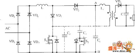
View full Circuit Diagram | Comments | Reading(892)
The PFC converter circuit of I3 parallel connected single-stage Boost type
Published:2011/7/7 4:38:00 Author:Seven | Keyword: PFC converter, single-stage
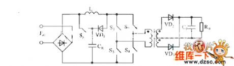
View full Circuit Diagram | Comments | Reading(544)
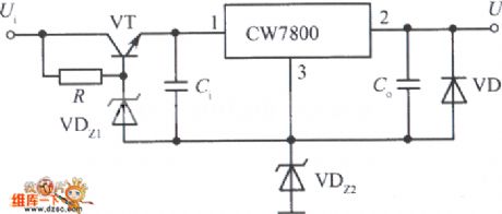
Fixed negative output integrated voltage stabilizer circuit with the input port short-circuit protection function
Published:2011/7/6 21:38:00 Author:Christina | Keyword: Fixed, negative output, integrated voltage stabilizer, input port, short-circuit protection
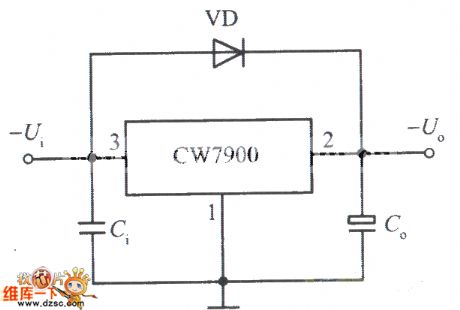
View full Circuit Diagram | Comments | Reading(699)
Positive and negative output voltage integrated voltage stabilization power supply circuit
Published:2011/7/7 1:58:00 Author:Christina | Keyword: Positive, negative, output voltage, integrated, voltage stabilization, power supply
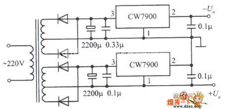
View full Circuit Diagram | Comments | Reading(632)
Light control integrated voltage stabilization power supply circuit (2)
Published:2011/7/7 2:03:00 Author:Christina | Keyword: Light control, integrated voltage stabilization, power supply circuit
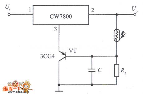
View full Circuit Diagram | Comments | Reading(551)
YDS100/200 switching power supply integrated circuit
Published:2011/7/7 2:53:00 Author:Christina | Keyword: switching power supply, integrated circuit
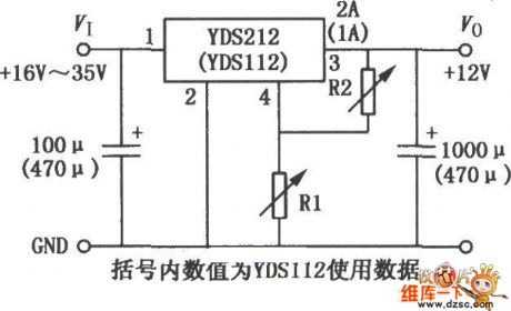
Figure:YDS100/200 switching power supply integrated circuit
(View)
View full Circuit Diagram | Comments | Reading(668)
Large current output integrated voltage stabilization power supply circuit (1)
Published:2011/7/7 3:13:00 Author:Christina | Keyword: Large current, output, integrated voltage stabilization, power supply
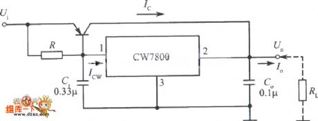
View full Circuit Diagram | Comments | Reading(497)
Constant current source circuit composed of the three-port fixed output integrated regulator
Published:2011/7/7 3:53:00 Author:Christina | Keyword: Constant current, source, three-port, fixed, output integrated regulator
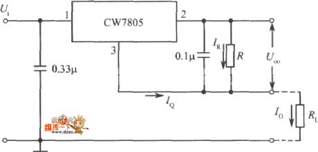
View full Circuit Diagram | Comments | Reading(722)
High input-high output integrated voltage stabilization power supply circuit (1)
Published:2011/7/7 20:22:00 Author:Christina | Keyword: High input, high output, integrated, voltage stabilization, power supply
View full Circuit Diagram | Comments | Reading(540)
landlines of power supply circuit
Published:2011/7/5 0:57:00 Author:chopper | Keyword: landlines, power supply circuit
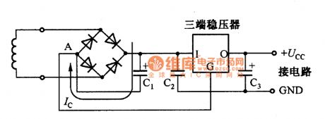
The power supply circuit is a high-power circuit,we should pay attention to the down-lead,or it will not gain low-noise supply.The picture is the positive supply circuit formed by full-wave rectification and three terminal regulator.In the circuit,the ground of smoothing capacity C1 and regulator is connected to point A. Point A is a reference potential.The landlines of regulator will effect a lot to the circuit performance.If there is noise or hun in the landlines,it will emerge on the output end.There is smoothing current Ic charged and discharged by capacitor through The landlines of smoothing capacity C1.The capacity C2 is a vibration control capacity.
(View)
View full Circuit Diagram | Comments | Reading(607)
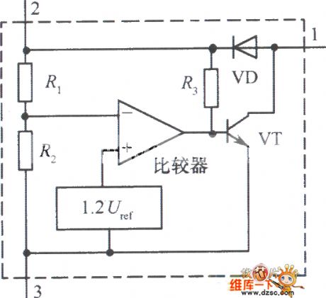
MIC5158 battery charger circuit
Published:2011/6/23 10:10:00 Author:chopper | Keyword: battery charger circuit
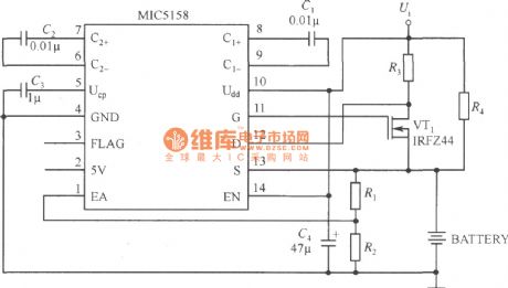
The constant-current charge circuit of MIC5158 is shown as the following picture.This circuit offers a constant current during the charging process(35mV/R3) until the voltage Uf1 is equal to 1.235(1+R1/R2).As for the formula,Uf1 is floating charge voltage(V).MOSFET tube will be cut off when the circuit reaches the floating charge voltage.Charge current is offered by R4. (View)
View full Circuit Diagram | Comments | Reading(1023)
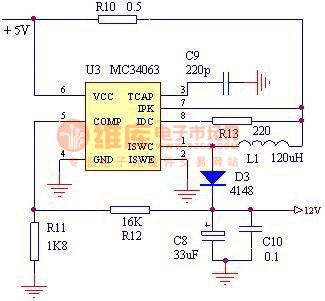
5v to 12v step-up circuit
Published:2011/6/16 5:12:00 Author:Borg | Keyword: step-up circuit
View full Circuit Diagram | Comments | Reading(2412)
The 2-line mains auto converting power supply device circuit
Published:2011/7/4 4:00:00 Author:Borg | Keyword: power supply, converting
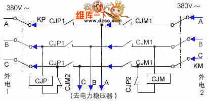
Generally, the 2-line supply device circuit has manual converting control, however, due to the bad weather in mountains, power-off often happens, and the people on duty are more than 100m far away from the power room, once one line is cut off, it will take a long time to inverse the power by people, the labor intensity is high, and the TV emitter and the 3 set of FM broadcasts are stopped, which affects the broadcast. This auto power converting equipment can convert power in 1/10S when one line of power is broken down suddenly, which can keep the broadcast out of effect. The whole equipment is cooperating with the power stabilizer(250KVA).
(View)
View full Circuit Diagram | Comments | Reading(555)
TL431 high-power adjustable circuit diagram
Published:2011/7/1 1:48:00 Author:Ecco | Keyword: high-power , adjustable
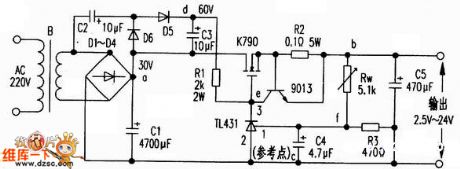
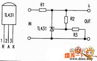
Precision voltage reference IC TL431 with T0-92 package is shown as the Figure 1. Its performance is continuously adjustable output voltage which is up to 36V, and the operating current range is 0.1. 100mA typical dynamic resistance is 0.22 Ω, and it has low output noise. Figure 2 is the typical application of the TL431, of which both ends of ③, ② feet output voltage V = 2.5 (R2 ten R3) V/R3. If you change the size of the resistance of R2, you can change the size of the output reference voltage. D5, D6, C2, C3 form the doubler circuit.
(View)
View full Circuit Diagram | Comments | Reading(5181)
DC / DC converter 250W switching power supply circuit diagram composed of TOP249Y
Published:2011/6/30 3:05:00 Author:Ecco | Keyword: DC / DC , converter, 250W , switching power supply
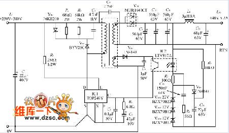
The DC / DC converter switching power supply uses a TOP249Y with input 250V ~ 380V DC, and the output is 48V, 5.2A (250W), then the power efficiency is up to 84%. The circuit is shown in Figure 2. High-frequency filter capacitor C1 is specifically inhibit the input from the electromagnetic interference. As the TOP249 works in its power limit, which need short connect X-side and the source S, within the limit is set the maximum current, that is ILIMIT = ILIMIT (max) = 5.7A.
(View)
View full Circuit Diagram | Comments | Reading(6836)
The button recharging Li icon battery charge circuit
Published:2011/7/4 4:08:00 Author:qqtang | Keyword: button, Li icon, battery charge
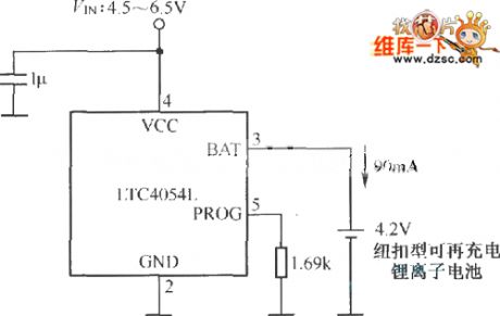
View full Circuit Diagram | Comments | Reading(601)
The internal circuit of the low voltage special integrated chip MC3X164
Published:2011/7/4 4:10:00 Author:qqtang | Keyword: internal circuit, low voltage, special integrated chip
View full Circuit Diagram | Comments | Reading(566)
The power supply circuit of bridge sensor
Published:2011/7/4 22:56:00 Author:Lucas | Keyword: power supply , bridge sensor
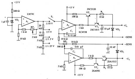
In the circuit, the maximum input voltage of A2 is ± 10V, and the + lOV reference voltage can be got by Al, and the voltage stability is decided by the regulator diode VDI. Thus, VDl uses temperature compensated voltage regulator diode 1S2192. S1 switches A2's input voltage to get different input voltages with±10V, 5V, ± 2.5 V, ±1.25 V by connecting to different resistors. A2 is the non-inverting amplifier, and the output gets positive voltage + U. ; A3 is the inverting amplifier, and the output gets negative voltage -U. ; RP2 is used to adjust the negative output voltage.
(View)
View full Circuit Diagram | Comments | Reading(1165)
DC power on / off switch circuit
Published:2011/7/4 22:09:00 Author:Lucas | Keyword: DC power , on-off switch
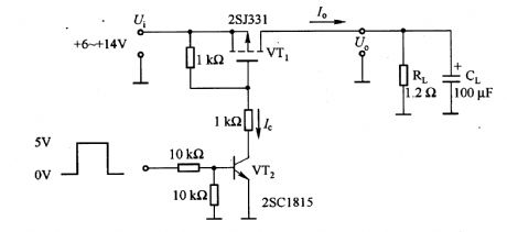
It is the switch circuit with the input voltage in +6 to +14 V, load current I in lOA. Minimum input voltag is decided by the used MOSFET (VTl) gate threshold voltage. VT2 collector current is decided by the required switching speed. If it uses P-channel power MOSFET, the gate resistance can be high because of IC being small, so the current consumption can be low. If the open speed is faster, the drain current is large. When conditions are bad, it can be connected capacitor between gate - source pole of VTl.
(View)
View full Circuit Diagram | Comments | Reading(8544)
100W VMOS FET inverter power supply circuit diagram
Published:2011/7/1 1:27:00 Author:Ecco | Keyword: 100W , VMOS, FET , inverter
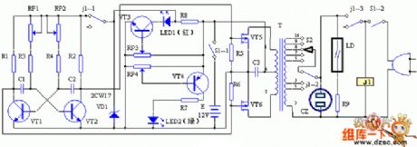
Working principle is shown in Figure 1 (click to download the schematic). VT1 and VT2 constitute a multivibrator oscillator with the oscillation frequency in 5Hz. When the voltage drops, the oscillator is provided by the regulator VD1 to keep the same frequency. Multivibrator outputs square wave voltage to drive VMOS high-power tube directly, then the 220V AC is led from the outlet CZ after boosted by step-up transformer. Relay J1 is used for automatical convertion in charging and inverter. LED1 indicates the end of the charging, LED2 is discharged instruction.
(View)
View full Circuit Diagram | Comments | Reading(2254)
| Pages:196/291 At 20181182183184185186187188189190191192193194195196197198199200Under 20 |
Circuit Categories
power supply circuit
Amplifier Circuit
Basic Circuit
LED and Light Circuit
Sensor Circuit
Signal Processing
Electrical Equipment Circuit
Control Circuit
Remote Control Circuit
A/D-D/A Converter Circuit
Audio Circuit
Measuring and Test Circuit
Communication Circuit
Computer-Related Circuit
555 Circuit
Automotive Circuit
Repairing Circuit