
Index 191
Practical nickel cadmium battery automatic charger circuit
Published:2011/7/13 22:12:00 Author:TaoXi | Keyword: Practical nickel cadmium battery, automatic charger

The charge which is introduced in this article can supply the stable charging current and it has the timing circuit to control the charging time.
As the figure 4-17 shows, when the press the button SW1, the city electricity is connected, the relay RL1 closes, the red light emitting diode LED2 turns on, this means that the charger has connected with the power. The regulator IC5 supplies the 12V DC voltage to the RL1. The regulator IC2 supplies the +5V voltage to the logic circuit. The constant current source is composed of IC1, it can output the stable charging current. R1 fixes the charging current at 50mA (used to charge the LR06 type storage battery), R6 fixes the charging current at 11mA (used to charge the 9V 6F22 type laminated battery).
(View)
View full Circuit Diagram | Comments | Reading(736)
Practical simple battery automatic charger circuit
Published:2011/7/13 22:37:00 Author:TaoXi | Keyword: Practical, simple, battery, automatic charger

The circuit principle of the charger is as shown in figure 4-18. The 220V AC city electricity is transformed, rectified and filted by this circuit to output the 20V direct current, and this current charges the battery through the three-port voltage stabilizer. The switching circuit TWH8778 can be used to detect the two-end voltage of the battery.
When the charging starts, the voltage of battery is not enough to conduct the TWH8778, the equivalent circuit is as shown in figure 4-19(a). The constant current charges the battery, the constant current value I0=12.5/R, R is one resistance value of the R1-R4. When the battery voltage increases to the set value, the circuit of figure 4-19(b) is automatically converted into the circuit of 4-19(c).
(View)
View full Circuit Diagram | Comments | Reading(787)
Automatic charging, power supply dual-use device circuit
Published:2011/7/13 22:58:00 Author:TaoXi | Keyword: Automatic, charging, power supply, dual-use, device circuit

Operating principle:
The circuit is as shown in figure 4-3, this device uses three pieces of integrated circuits: IC1 is the LM317, the adjustable voltage stabilization power supply is composed of LM317 and other surrounding components, the adjustment range is 1.25V-15V; IC2 is the pulse oscillator which is composed of the time base circuit 555, the duty ratio is 60%; IC3 is the high current and low current charging and discharging conversion control circuit.
After you pressing the button AN, the battery voltage is lower than the gate voltage of D, so D outputs the high level, the transistor V4 conducts, the relay K closes to form the self-protection.
(View)
View full Circuit Diagram | Comments | Reading(686)
New depolarization nickel cadmium battery automatic charger circuit
Published:2011/7/13 20:00:00 Author:TaoXi | Keyword: New, depolarization, nickel cadmium battery, automatic charger
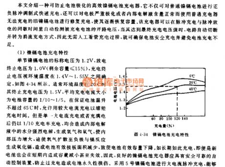
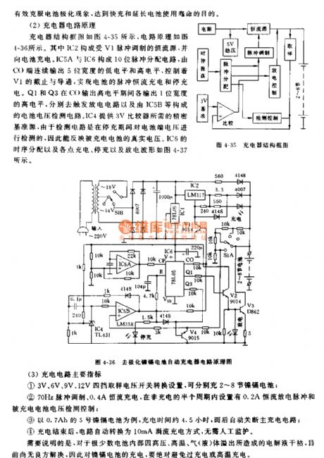
The structure diagram of the charger is as shown in figure 4-35, the circuit principle is as shown in figure 4-36. The constant current source which is modulated by the V pulse is composed of IC2, it charges the battery. The 10-bit pulse distribution circuit is composed of the IC5A and IC6, the Co port continuously outputs the low level and high level with 5-bit width to control the cut-off and conduction of V1 and this method realizes the constant current pulse charging and stop-charging of the battery. Q1 and Q3 output the high levels with 1-bit width when the Co outputs the high level, and the 1-bit high levels trigger the battery voltage detection circuit which is composed of the IC5B and the discharging current respectively. IC4 supplies precision reference source which is needed by the 3V comparator.
(View)
View full Circuit Diagram | Comments | Reading(619)
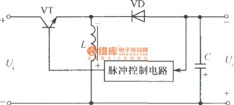
Practical circuit of the step-down chopper type switching voltage stabilization power supply
Published:2011/7/12 0:48:00 Author:TaoXi | Keyword: Practical circuit, step-down, chopper, switching, voltage stabilization, power supply

The practical circuit of the step-down chopper type switching voltage stabilization power supply is as shown in the figure. The VT1 is the adjusting switching tube, the VT2 and VT3 are the two-stage switching tube. The VD1 and VD2 which are connected with the two promote tubes' emitters can be used to prevent the reverse breakdown of the transistor emitter junction. The conduction and cut-off time of VT1 are decided by the self-excited multivibrator which is composed of the VT5 and VT6, the VT4 emitter follower plays the isolation and amplification functions. The flip time of the multivibrator depends on the emitter-coupled differential amplifier which is composed of VT7 and VT8.
When the output voltage range of this circuit is ±20%, the input voltage range is in the range of ±0.5%, the efficiency is 93%.
(View)
View full Circuit Diagram | Comments | Reading(1696)
Polarity transform type and chopped type switching voltage stabilization power supply principle diagram
Published:2011/7/12 1:02:00 Author:TaoXi | Keyword: Polarity transform, chopped type, switching, voltage stabilization, power supply, principle diagram
The polarity transform type and chopped type switching voltage stabilization power supply principle diagram is as shown in the figure. When the switching adjustment component transistor VT is in the conduction state, the input voltage Vi adds to L to produce the current, the diode VD cuts off reversely. When the transistor VT is cutting off, the current of inductance L decreases gradually, the polarity of the induced electromotive force is as shown in the figure. This induced electromotive force conducts the diode VD to charge the capacitance C, the polarity of the output voltage Vo of the capacitance C is opposite with the input voltage Vi. When the voltage of the load will fall, the capacitance C discharges the load again. The output voltage Vo will higher than the input voltage Vi.
(View)
View full Circuit Diagram | Comments | Reading(633)
Width modulation, frequency modulation hybrid type switching power supply (1)
Published:2011/7/12 1:16:00 Author:TaoXi | Keyword: Width modulation, frequency modulation, hybrid type, switching, power supply

The self-excited oscillation of this circuit is realized by the R13C1. When the power is starting, the 220V AC adds to the primary stage of the transformer T1, and it is secondary transformed, bridge type rectified and filted by this circuit, then the capacitance C6 outputs the 15V unstable smooth DC voltage to add to the input ports of the complex switching power transistors VTl2~VT14; at the same time, this voltage supplies the stable operating voltage for the integrated voltage regulator W724 through the resistor R10 and the regulator VD6. Becasue the output voltage Vo has not established, so the two ends of the sampling voltage divider resistors R17, R24, R18 has no voltage, the VT5 of the error amplifier cuts off because there is no base electrode bias voltage.
(View)
View full Circuit Diagram | Comments | Reading(569)
Width modulation, frequency modulation hybrid type switching power supply (2)
Published:2011/7/12 1:34:00 Author:TaoXi | Keyword: Width modulation, frequency modulation, hybrid type, switching, power supply

The control circuit is composed of the VT902~VT904. When the power supply is working, the induced voltage of the transformer T901's sampling windings ⑦~⑧ is rectified by the diode VD911 to supply to the error amplifier for the sampling amplification. The error voltage outputs from the collector electrode to the base electrode of VT903 to control the VT903's bias voltage. And the output pulse of the ⑦ ~ ⑧ end-windings is differentiated by the R919 and C913 to add to the base electrode of VT903. The two signals is superimposed to control the conduction and cut-off of VT902 and VT903. When the two tubes is cut-off, the rectangular pulse voltage of the feedback winding ⑨~⑩ ports is rectified by VD901 to establish the composite voltage on the capacitor C910, so the VD910 is anti-bias cut-off, the VT901 conducts.
(View)
View full Circuit Diagram | Comments | Reading(648)
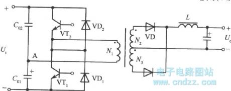
Capacitive voltage divider type clamping single-ended flyback type switching power supply
Published:2011/7/12 1:47:00 Author:TaoXi | Keyword: Capacitive, voltage divider type, clamping, single-ended, flyback type, switching, power supply

The capacitive voltage divider type clamping single-ended flyback type switching power supply is as shown in the figure. When the VT1 is in the conduction state, the capacitance C02 charges, the COl discharges, the circuit adds the 1/2 input voltage to the original edge winding N1l of the transformer T1; when the VTl is in the cut-off state, the voltage polarity of Nll reverses, when the collector-emitter voltage Ucel of VT1 reaches the input voltage Vi, the diode VD4 conducts, the Ucel is clamped; similarly, when the VT2 is in the conduction state, the C02 discharges, the C0l charges, the circuit adds the 1/2 input voltage to the original edge winding N2l of the transformer T2; when the VT2 is in the cut-off state, the voltage polarity of N2l reverses, after the VD3 is conducted, the Uce2 is clamped by the input voltage Vi.
(View)
View full Circuit Diagram | Comments | Reading(943)
The wSl57 and WSl06
Published:2011/7/12 1:59:00 Author:TaoXi


The appearances and the pin arrangements of the wSl57 and WSl06 are as shown in figure (a) and (b).
Both of them belong to the surface installation component (SMC), they have different package types and pin numbers. In fact the WSl57 only has three pins, it belongs to the three-port component. D is the drain electrode of the MOSFET, the C is the control port, the S is the source electrode. The WSl06 uses the SMD-8 package, it has six S poles, the rest of the poles are the D pole and C pole, so it is still the three-port component. The wSl57 and WSl06 have the same internal circuit. The internal block diagram of the WSl57 is as shown in the figure, it is composed of the l00kHz oscillator, the reference voltage source, the PWM comparator, the control circuit, the driver stage, the power switch tube and the undervoltage, overcurrent and thermal protection circuits.
(View)
View full Circuit Diagram | Comments | Reading(741)
VMOS tube switching power supply (1)
Published:2011/7/12 2:09:00 Author:TaoXi | Keyword: VMOS tube, switching power supply

The stabilized voltage power supply circuit which uses the VMOS tube as the switch device is as shown in the figure. In this figure, the VT5 is the VMOS power transistor, it is the switch adjustment device of this power supply; the L1 is the energy storage inductance; VD3 is the free-wheeling diode, VT3 is the MOSFET which can be used as the constant current source of VTl and VT2 to supply the 1mA constant current for the emitters; Cl is the input filter capacitance; C5, C6 and C7 are the output filter capacitances.
In order to reduce the power consumption of the switching adjustment tube VT5 and improve the flip speed of it, this circuit uses the bootstrap network which is composed of the R5 and C4. When the VT5 is in the cut-off state, the source potential is 0V, the input voltage charges the C4 through the resistor R4 of the diode VD2, so the voltage of C4 closes to the input voltage. (View)
View full Circuit Diagram | Comments | Reading(944)
VMOS tube switching power supply application circuit (3)
Published:2011/7/12 2:33:00 Author:TaoXi | Keyword: VMOS tube, switching, power supply, application circuit

The VMOS tube switching power supply application circuit is as shown in the figure, it is designed as one kind of push-pull switching power supply which uses the TL494 switch integrated circuit component as the control circuit.
In the figure, the TL494 is used as the control circuit of the power supply, in addition to being the oscillation outside source, it is also responsible for the task of adjusting and stabilizing the output voltage. The oscillation frequency is decided by the external components R1 and C1. The switching frequency of this power supply is 100kHz. The VD1 and VD2 are the isolation diodes, the operating voltage is 33V. T is the push-pull output transformer, the primary center tap of it is connected with the DC 12V input power supply. The secondary stage is connected with the output bridge rectifier circuit. The output filter is composed of the current choking coil and the filter capacitance C3.
(View)
View full Circuit Diagram | Comments | Reading(8276)
Practical circuit of the half-bridge type switching voltage stabilization power supply
Published:2011/7/12 3:14:00 Author:TaoXi | Keyword: Practical circuit, half-bridge, switching, voltage stabilization, power supply

The practical circuit of the half-bridge type switching voltage stabilization power supply is as shown in the figure. The half-bridge type converter is composed of the VTl, VT2, T2, C6 and C7. The control signal is amplified by the VT3 and VT4, and it drives the switching tubes VT1, VT2 to alternately turn on and off through the transformer T1. The two ends of the T2's primary coil is connected with the midpoint of C6, C7 and the midpoint of VTl, VT2, so it can couple the power signal to the secondary stage of T2. And it outputs the stable DC through the VDl6, VDl7 full-wave rectification and the L6, C28 two-stage filtering.
The control circuit uses three dual NAND gate ICs as the main part. The JD2 is the timer, it produces the 20kHz square wave. The two monostable triggers are composed of the JD3 and JD4, and the two monostable triggers form the pulse width regulator.
(View)
View full Circuit Diagram | Comments | Reading(670)
Half bridge type converter power supply circuit
Published:2011/7/12 3:42:00 Author:TaoXi | Keyword: Half bridge type, converter, power supply
In the high voltage switch power supply, we usually use the half bridge type converter circuit if the output power is large. The circuit is as shown in the figure. It is composed of two capacitances and two high voltage transistors. When the two transistors are cut-off, if the capacities of the two capacitances are the same and the circuit is symmetrical, the voltage of the capacitance midpoint A is the half of the input voltage. When the VTl is conduction, the capacitance C01 discharges through the VTl and the primary winding N1 of the transformer; at the same time, the capacitance C02 charges through the input power supply, the VTl and the original edge winding N1 of T1. In the process of charging and discharging, the electric potential of midpoint A will reduce exponentially.
(View)
View full Circuit Diagram | Comments | Reading(1572)
Non-isolated silicon controlled switching power supply
Published:2011/7/12 4:07:00 Author:TaoXi | Keyword: Non-isolated, silicon controlled, switching, power supply
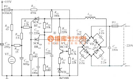
The non-isolated switching power supply which is composed of the silicon controlled is as shown in the figure. The 220V AC voltage adds to the bridge type rectifier which is composed of the VD503, WD505, VD507, VD509 directly. The full-wave voltage that is output by it adds to the cathode of the adjustment device SCR529 through the current choking coil, you can change the output voltage by changing the phase position of the SCR529 trigger pulse. The output voltage is filted by the two-stage RC filter which is composed of the R544, C535 and R545, R546, C536 and it will change into the 155V smooth DC. The VT516 is the error amplifier tube. The VD518 is the zener diode which supplies the reference voltage to the VT516. The sampling voltage divider circuit is composed of the R531, R515, R514.
(View)
View full Circuit Diagram | Comments | Reading(1261)
The practical circuit of the non-isolated switching power supply
Published:2011/7/12 4:27:00 Author:TaoXi | Keyword: practical circuit, non-isolated, switching, power supply

The practical circuit of the non-isolated switching power supply is as shown in the figure, it can be used as the switching power supply of the MuDan TC--483D type color TV set, it is composed of the grid filter which is composed of the C80l, C802, L801; the bridge rectifier circuit which is composed of the VD80l and VD802; the filter which is composed of the R802 and C807, the peak voltage limiter which is assumed by the piezoresistor VD811, the pulse oscillator which is composed of the switch tube VT80l and the pulse transformer T801; the pulse width modulator which is composed of the VT802; the error amplifier which is composed of the VT803.
(View)
View full Circuit Diagram | Comments | Reading(643)
MC33370
Published:2011/7/12 4:45:00 Author:TaoXi

The MC33370 series uses the 8-pin dual-row DIP package (DIP8) or the 5-pin TO (View)
View full Circuit Diagram | Comments | Reading(839)
The DPCA-Fukang DC7140 image symbol circuit
Published:2011/7/12 0:22:00 Author:Borg | Keyword: DPCA-Fukang, image symbol
Figure: The DPCA-Fukang car circuit diagram1-wire wielding connector; 2-plug connector; 3-connector contactor; 4-connector contactor with marks; 5-fixed connector; 6-fixed connector; 7-wire wielding ground connection; 8-connector ground connection; 9-part shell ground connection; 10-switch (with auto reset); 11-hand switch; 12-converting switch; 13-normally open contactor(auto reset); 14-normally closed contactor (auto reset); 15-hand switch; 16-mechanical switch. (View)
View full Circuit Diagram | Comments | Reading(5060)
IX0689 power supply
Published:2011/7/12 19:29:00 Author:TaoXi | Keyword: power supply

The 300V DC voltage is divided by the R707 and R724, and then this 300V DC voltage adds to the pin-12 of the N701 through the C735 and L701, the pin-12 of the IX0689 is the B port of the internal switching tube, so the switching tube conducts, the current gets in this circuit through the C port of the pin-15, and it gets out through the E port of the pin-13.
The pin-3 and pin-5 of the T701 is the positive feedback winding, when the switching tube is conducting, the pin-5 has the positive polarity and the pin-3 has the negative polarity, the voltage of pin-5 adds to the pin-12 of N701 through the V735, R713 and L701 to increase the current of the switching tube, so this cycle makes the switching tube saturate quickly.
(View)
View full Circuit Diagram | Comments | Reading(1400)
Small power switching power supply circuit produced by the CWl840
Published:2011/7/12 19:34:00 Author:TaoXi | Keyword: Small power, switching, power supply

View full Circuit Diagram | Comments | Reading(720)
| Pages:191/291 At 20181182183184185186187188189190191192193194195196197198199200Under 20 |
Circuit Categories
power supply circuit
Amplifier Circuit
Basic Circuit
LED and Light Circuit
Sensor Circuit
Signal Processing
Electrical Equipment Circuit
Control Circuit
Remote Control Circuit
A/D-D/A Converter Circuit
Audio Circuit
Measuring and Test Circuit
Communication Circuit
Computer-Related Circuit
555 Circuit
Automotive Circuit
Repairing Circuit