
Index 185
Circuit of using solar to charge to battery
Published:2011/5/13 3:07:00 Author:Nicole | Keyword: solar, battery
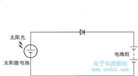

The output current of solar battery is influenced by weather condition:
(View)
View full Circuit Diagram | Comments | Reading(590)
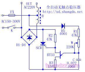
Automatical noncontact AC regulator circuit
Published:2011/5/13 2:44:00 Author:Nicole | Keyword: AC regulator
This circuit can adjust output voltage accurately and fast, when mains supply voltage is in the range of 150V~300V.
The circuit is shown as below, after mains supply enters VD1~VD4 full-bridge rectifier by L1, it is added to SCR VT, the conduction angle of VT is controlledbyBT33. A relaxation oscillator is composed of BT33, C, R1, R2, R3, and KP, changing KP can change the oscillation period. When the mains supply voltage rises, the voltage on BT33 rises too, the oscillation becomes quick, the VT conduction angle decreases, the voltage on VT rises, the voltage on L1 dose not change; on the contrary, the voltage on VT drops, the voltage on L1 dose not change; thus the voltage coupled by L2 remains constant. Because it adopts full-bridge rectifier, so the voltage on L1 and L2 are all sine wave.
The current of D1~D4 and VT depends on the capacity of transformer, it should have lager capacity, the compression should be more than 600V, R1 and R2 choose 3W resistance, KPhad batterselectmore than2W adjustable resistance.
(View)
View full Circuit Diagram | Comments | Reading(1866)
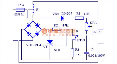
Automatical noncontact regulator circuit
Published:2011/5/13 2:44:00 Author:Nicole | Keyword: noncontact regulator
This regulator has no contact, its voltage regulation is precise and fast, the range of application is wide: AC150V~AC300V.
Principle: mains supply enters D1~D4 full-bridge rectifier by L1, it is added to SCR, the conduction angle of SCR is controlled by BT33. A relaxation oscillator is composed of BT33, C, R1, R2, R3, and W, changing W can change the oscillation period. When the input voltage rises, the voltage on BT33 rises too, the oscillation becomes quick, the SCR conduction angle decreases, the voltage on SCR rises, the voltage on L1 is changeless; on the contrary, the voltage on SCR drops, the voltage on L1 dose not change; thus the voltage coupled by L2 remains constant. Because it adopts full-bridge rectifier, so the voltage on L1 and L2 all keep sine wave.
The components selection: the current of D1~D4 and SCR depends on the capacity of B, it should have lager capacity, the compression should be more than 600V, R1 and R2 choose 3W resistance, W had better select more than 2Wadjustable or potentiometer. (View)
View full Circuit Diagram | Comments | Reading(796)
Integration orthogonal detector circuit used in LED
Published:2011/5/11 8:52:00 Author:Nicole | Keyword: detector, LED
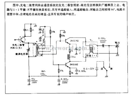
In figure, photodiode array is irradiated by LED of communication system, converting the optical information into broadcast band. The circuit is similar to 1:1 balance-disbalance converter, it has single-channel input, two-channel output, the phase shift between two output is 90 degrees. This circuit does not require neutralizing, it can give high gain reasonably and has low noise. (View)
View full Circuit Diagram | Comments | Reading(680)
Pointed pulse detection circuit
Published:2011/5/11 8:48:00 Author:Nicole | Keyword: pointed pulse, detection
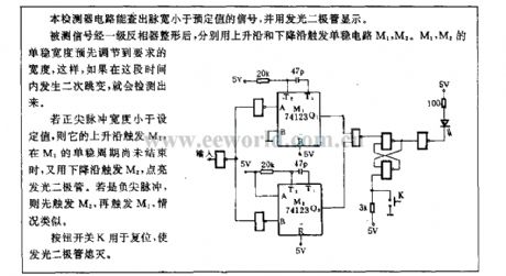
This detector circuit can detect the singal,the pulse width of this singalis smaller than the predetermined value, and displayed by LED.
After plastic by primar inverter, the tested signal uses rising edge and falling edge to trigger monostable circuit M1, M2. The monostable width of M1, M2 is adjusted to requested previously, so if it occurs second jumping, it will be detected.
If the positive pointed pulse width is smaller than set value, its rising edge trigger M1, when the monostable cycle of M1 is not finished,M2 is triggered by the falling edge, LED is lighted up. If it is negative pointed pulse, triggering M2 first, then trigger M1, the situation is similar.
The push-button switch K is used to reset, and to put out LED. (View)
View full Circuit Diagram | Comments | Reading(679)
Light change detector drive relay circuit
Published:2011/5/11 8:45:00 Author:Nicole | Keyword: detector drive, relay
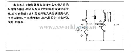
This circuit adopts electric capacity coupling between phototransistor and bipolar transistor, so it only has influence on the intermission or fast change of light, it has no effect on the slow change of ambient light produced by cloud or sunrise. When there is flashing, the relay pulls in; and if there is no light, it will release. (View)
View full Circuit Diagram | Comments | Reading(603)
Photosensitization
Published:2011/5/11 8:37:00 Author:Nicole | Keyword: photosensitization
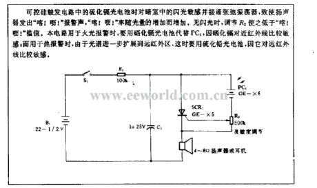
The cadmium sulfide photocell of thyristor trigger circuit is sensitive to the flashing in dark room and it is connected to relaxation oscillator, it leads to the loudspeaker souds out alarm, its alarm frequency increases with the increasing of the light density. When it is no flashing, R2 will be lower than the threshold value after adjusting. When this circuit is used for firelight alarming, it should use cadmium selenide to replace PC1, because cadmium selenide is sensitive to near infrared ray; when this circuit is use to heat alarm, because the spectrum is further expanded to far infrared band, so it should use pbs photocell due to it is sensitive to far infrared ray. (View)
View full Circuit Diagram | Comments | Reading(581)
Output record circuit of photoelectric multiplier
Published:2011/5/11 8:26:00 Author:Nicole | Keyword: output record, photoelectric multiplier
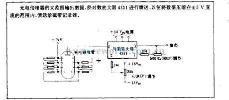
The large range output data of opto-electrical multiplier is fed by logarithmic amplifier 4351, the data is compressed into the range of ±5V DC, then it is fed to tape recorder. (View)
View full Circuit Diagram | Comments | Reading(616)
Photoelectric lighting circuit
Published:2011/5/11 8:17:00 Author:Nicole | Keyword: photoelectric lighting circuit
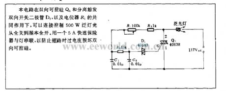
Under the action of TRIAC Q1 and separation trigger bidirectional switching diode D1 and potentiometer R1, this circuit can connect and control 500W light from all off to all on. 5A fast safety device is series connected with light, it can prevent TRIAC from damaging due to the short circuit. (View)
View full Circuit Diagram | Comments | Reading(678)
Optical receiver circuit
Published:2011/5/10 8:02:00 Author:Nicole | Keyword: Optical receiver
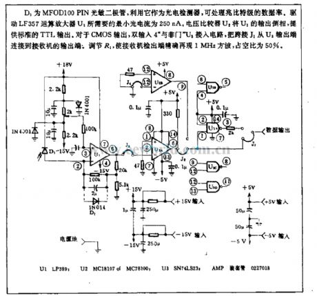
D1 is MFOD100 PIN photosensitive diode, using it as photodetector can deal with the data rate of Megabits Mb. The minimum photocurrent is 250nA which is needed by driving LF357 operation amplifier U1. U1's output is reversed phase by voltage comparator U2, it can provide standard TTL output. For CMOS output, double input 4 NAND gate U3 is connected into circuit, the bridge connection J1 is connected from U2 output terminal to receiver output terminal. To adjust R1, to make receiver take-off terminal accurate reappearance 1MHz square wave, the duty ratio is 50%. (View)
View full Circuit Diagram | Comments | Reading(700)
Full-bridge power convertor circuit diagram with increase output power
Published:2011/5/5 7:24:00 Author:Nicole | Keyword: Full-bridge power convertor
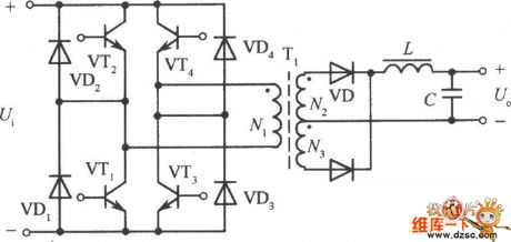
The two electrolytic capacitors of half-bridge converter circuit are changed to the other two high back pressure power transistors, and coupled with appropriate drive circuit then canformfull-bridge converter circuit, the figure is as shown. VT1, VT2, VT3, VT4 form 4 bridge arms. High frequency transformer T is connected between them. Relative VT1, VT4 and VT2, VT3 areinspired by the drive circuit, then theyturns onalternately, the DC input voltage into a high-frequency square-wave transform AC voltage. The course of working is the same as push-pull power converter circuit. Thus, when the high frequency transformer at work, the voltage of primary coil is considered to the supply voltage, it isone time ofthe half-bridge circuit output voltage, the pressure of each transistor remains at the supply voltage, twice the output power increases. If the current reaches half-bridge circuit, that means the current increases twice, then the output power can increase 4 times.
The main disadvantages of full-bridge circuit is that it needs 4 groups transistor base drive circuits which are insulative with each other, it enlarges the cost and complicates the control drive circuit.
(View)
View full Circuit Diagram | Comments | Reading(652)
Application circuit diagram of W296 with reset functions
Published:2011/5/5 7:16:00 Author:Nicole | Keyword: reset function
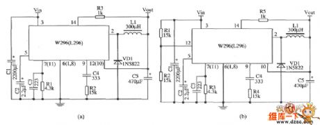
Compared with other switching regulator, W296 has a feature: internal reset function, when the regulator's output voltage produces reset signal within correct limits. The reset is achieved by the reset input side 12-pin, delayed side 13-pin and reset output side 14-pin. When the 12-pin voltage is lower than 5V, reset output is turned into low level by the comparator of resetting circuit; when the 12-pin voltage is higher than 5V, the reset output side turns into high level whichis delayed ashort period of time, the overtime is determined by the delay capacitor which is connected to 13-pin. The value of reset capacitor is between 1 ~ 4.7μF, when it is 2.2μF, the delay time is l00ms. The reset output side is a open collector, an external resistor is required when it is used. There are two ways, one is the 12-pin connects to output side directly, the other is to connect a resistor on input side, then divide to 12-pin, as shown. (a)connect output; (b)connect input.
(View)
View full Circuit Diagram | Comments | Reading(589)
Push-pull converter switching power supply circuit diagram
Published:2011/5/5 7:08:00 Author:Nicole | Keyword: switching power supply, push-pull converter
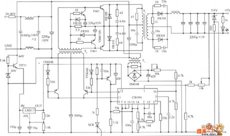
Push-pull converter switching power supply circuit. CW494 is a double-ended converter modulator integrated circuits, including error amplifier, voltage reference, clock oscillator, pulse width modulator and other circuits. Transformer T1 is a high-frequency transformer which can transferenergy to the load. T2 is incentive to promote the transformer. It can transmit the two series of drive pulse produced by the CW494 pulse modular to the drive and switch base of the push-pull circuit after amplfied by the driver transistor. L is the transformer windings on the pulse of the sample through the transformer and rectifier AC voltage, the resistance of the sample sent to the pulse modulation circuit CW494 16 feet, as the error amplifier inverting input. The power transistor of this power supply uses F461fast series. Where the voltage feedback, input and output are directly connected. If the input and output need to be isolated, the optocoupler can be used.
(View)
View full Circuit Diagram | Comments | Reading(4966)
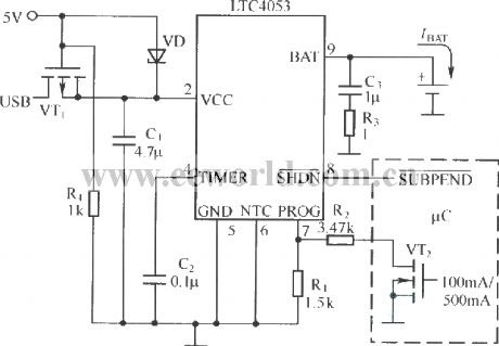
Practical USB interface lithium ion battery charger circuit(LTC4053 as controller)
Published:2011/5/13 3:57:00 Author:Nicole | Keyword: USB interface, lithium ion battery, controller, charger
View full Circuit Diagram | Comments | Reading(632)
LM7809-three terminal fixed steady voltage integrated circuit diagram
Published:2011/5/16 3:03:00 Author:Nicole | Keyword: three terminal, fixed steady voltage
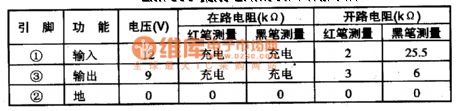
LM7809 is a three terminal fixed steady voltage integrated circuit which is produced by National Semiconductor Corporation, it can steady the input voltage to 9V, then it can provide the related circuits with it. It also can be applied to audio and video equipments, computer, display and all kinds of electrical appliances.
The pin function and data of LM7809 integrated circuit is shown in the table1, it is actually measured from Changhong ICN-l5 movement color television.
(View)
View full Circuit Diagram | Comments | Reading(589)
LM7812-three terminal fixed steady voltage integrated circuit diagram
Published:2011/5/16 2:57:00 Author:Nicole | Keyword: three terminal, fixed steady voltage
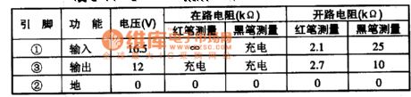
LM7812 is a three terminal regulator which is produced by National Semiconductor Corporation, as +12V steady voltage integrated circuit, it is widely used in all kinds of electrical appliances.
The pin function and data of LM7812 integrated circuit is shown in the table1, it is actually measured from Changhong CN-l5 movement color television.
(View)
View full Circuit Diagram | Comments | Reading(686)
ZC-2-10A 12v24v automatic charger circuit
Published:2011/5/13 4:27:00 Author:Nicole | Keyword: 24v automatic charger, 24v automatic charger
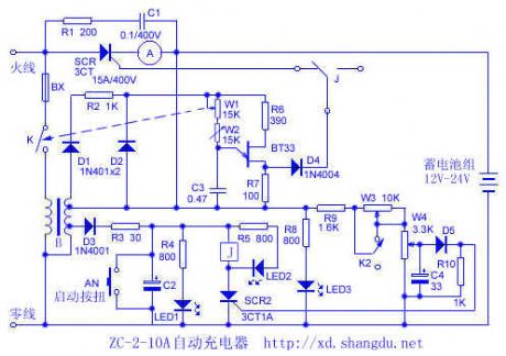
Relaxation oscillator is composed of unijunction transistors BT33、C3、W1、W2 and some other components, the produced pulse singal is transported to control pole of SCR1 by isolating diode D4, the trigger conduction angle of SCR1 can be changed by adjusting W1's resistance, it also changes the changing current. Storage battery fully charge automatic protection circuit is composed of SCR2, relay J, W3, W4, D5 and some other components, when the voltage on both sides of battery is charged to the upper limit which is set by W3, W4, then D5 turns on, SCR2 is triggered to turn on, LED2 displays, relay pulls in, J is switched to normally open, it cuts off SCR1's control pulse integrating, it stops charging to storage battey. K2 is the transfer switch of 12V, 24V changing batteries, as shown in the figure, it is in 12V gear.
(View)
View full Circuit Diagram | Comments | Reading(733)
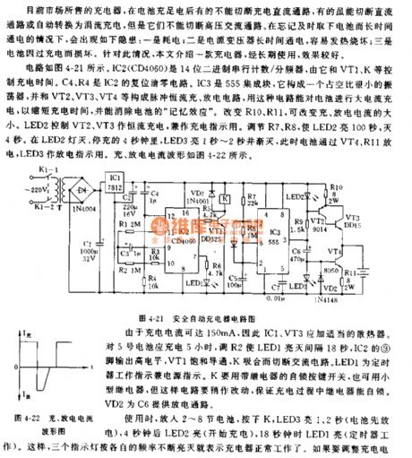
Safe and reliable multi-function charger circuit
Published:2011/7/18 20:09:00 Author:TaoXi | Keyword: Safe, reliable, multi-function, charger

The principle diagram of this charger is as shown in figure 5-16. The 220V city electricity is reduced by the transformer T, and it is bridge rectified by the diodes VD1-VD4 to output the 17V, 100Hz pulsating DC voltage, this DC voltage can supply the power to the charging circuit. The DC current is stabilized by IC1 to supply power to the time-base integrated circuit IC2(NE555), so the IC2(NE555) produces the oscillation, we can use the pulse signal which is output by the pin-3 to control the conduction and cut-off of the darlington tube which is composed of the VT1 and VT2. This circuit has the RP, the electric potential of the adjustable port of it can be used to set the recharging the battery benchmark voltage.
(View)
View full Circuit Diagram | Comments | Reading(665)
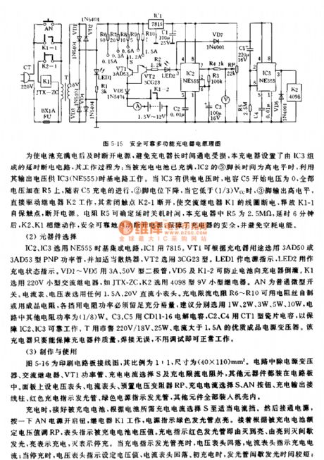
Safe automatic nickel cadmium battery charger circuit
Published:2011/7/18 19:56:00 Author:TaoXi | Keyword: Safe, automatic, nickel cadmium battery, charger
The circuit is as shown in figure 4-21. The IC2(CD4060) is the 14-bit binary serial counter/frequency divider, the IC2(CD4060) and the VT1, K control the charging time. The C4, R4 are the reset circuit of IC2. IC3 is the 555 manifold block, it forms the oscillator which has small duty ratio, and the pulse constant current charging and discharging circuit is composed of the IC3, VT2, VT3 and VT4. By using this kind of circuit, we can charge the battery with large current to shorten the charging time and eliminate the memory effect of the battery. By changing the R10 and R11, we can change the charging and discharging current. LED2 controls the VT2 and VT3 to do the constant current charging.
(View)
View full Circuit Diagram | Comments | Reading(1050)
Commonly used slow charger circuit principle diagram
Published:2011/7/18 19:41:00 Author:TaoXi | Keyword: Commonly used, slow charger, circuit, principle diagram
The 220V voltage is limited by the capacitor C1 and rectified by the diode to become the pulsating current, this pulsating current achieves the purpose of battery charging and charging indication through the batteries and ED network. Because the capacitor capacitive reactance is larger than the charging loop impedance, the loop current is decided by the value of C1, so this charging mode is the constant-current type, the value of capacitor C1 is 0.47uF, the charging current is about 30mA. The ED network is the charging indication circuit, R2 has the shunting effect. The electrolytic capacitor C2 has the energy storage effect. The resistor R1 is the bleeder resistance of C1.
(View)
View full Circuit Diagram | Comments | Reading(613)
| Pages:185/291 At 20181182183184185186187188189190191192193194195196197198199200Under 20 |
Circuit Categories
power supply circuit
Amplifier Circuit
Basic Circuit
LED and Light Circuit
Sensor Circuit
Signal Processing
Electrical Equipment Circuit
Control Circuit
Remote Control Circuit
A/D-D/A Converter Circuit
Audio Circuit
Measuring and Test Circuit
Communication Circuit
Computer-Related Circuit
555 Circuit
Automotive Circuit
Repairing Circuit