
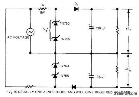
power supply circuit
Index 88
CRT_NUMBER_GENERATOR
Published:2009/7/16 21:35:00 Author:Jessie
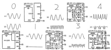
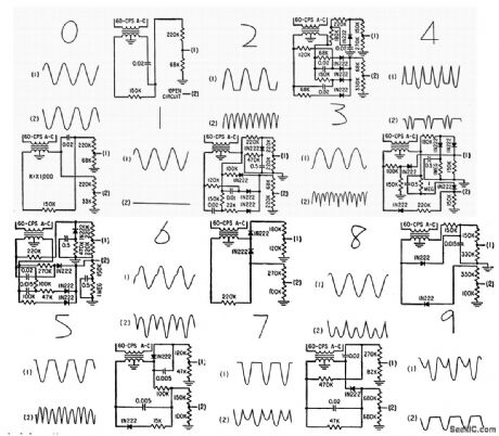
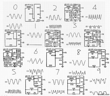
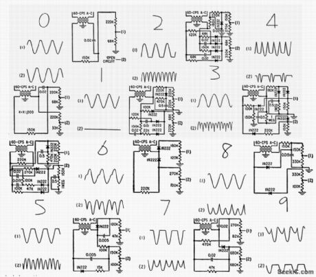
Lissajous patterns on crt form numerals 0 to 9 that appear to be handwritten. Vertical and horizontal waveshapes used to produce a number are continuously applied to pair of number gates. Gates open whom excited by high-voltage r-f transformer, permitting waveforms to pass through to crt defection plates and create problem on screen. All waveshapes are derived from 60-cps centertapped sine-wave source. Reliability is insured through use of passive elements (resistors, capacitors, and diodes) and standard techniques of dipping, limiting, and/or phase shifting to generate required waveshapes.-R. L. White, Forming Handwritten. Like Digits on CRI Display, Electronics,32:11, p 138-140. (View)
View full Circuit Diagram | Comments | Reading(984)
Bile Former Grade Power Circuit
Published:2011/7/17 23:37:00 Author:Felicity | Keyword: Bile Former Grade, Power Circuit

View full Circuit Diagram | Comments | Reading(706)
5_V_MICROPOWER_LINEAR_REGULATOR
Published:2009/7/16 21:35:00 Author:Jessie
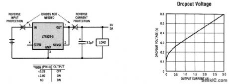
In battery systems where high load current is required intermittently and the system must remain in standby mode between uses, a linear regulator with micropower quiescent current and shut-down capability is needed. These situations arise in powering laptop disk drives, portable radio transmission modems, and peripheral motors, which are intermittently used. The LT1529 has 3 A current capability, 50 μA quiescent current, and just 16μA shutdown current. As shown in the circuit and chart, the LT1529-5 is a low-component-count solution with a very low dropout voltage of 0.6 V at 3-A output current. This low dropout is ideal for battery-powered systems in which extracting the maximum energy from the battery is important. In dropout, the output voltage will decrease smoothly, following the input. The quiescent current of the LT1529 increases only slightly in dropout, unlike the situation with many other low-dropout PNP regulators. (View)
View full Circuit Diagram | Comments | Reading(831)
BIOLOGICAL_SIGNAL_WAVEFORM_GENERATOR
Published:2009/7/16 21:35:00 Author:Jessie
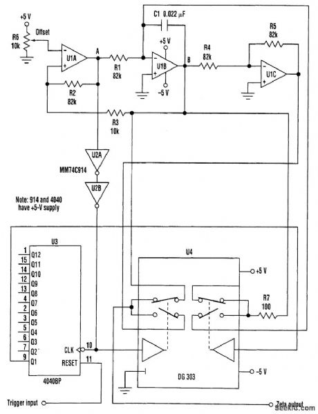
The circuit operates as follows: U1A and U1B form a triangle waveform generator, using R6 to offset the output so that it is a positive-going signal. The amplitude is set by R2 and R3, and the ramp's rate of rise is set by R1 and C1. Using the values shown, the output has an amplitude of >1 V with rise and fall times of 0.5 ms, giving a total zeta duration of 1 ms. U1C provides an inverted output of U1B. When the RESET pin on U3 is triggered, its Q1 output goes low and the short is removed across C1 by one half of the analog switch (U4). At this time, the output of U1A will be negative and the output of U1B will start to ramp up. During this time, the output of the circuit is taken from U1B via the other half of the analog switch. When the ramp reaches its positive voltage threshold, the output of U1A goes positive and U1B will start to ramp down. The output of U1A is taken via U2A and U2B (both inverting Schmitt triggers with special input circuitry that protects the input from negative voltages and allows them to level-shift) to the CLOCK input of U3. It is also taken to the analog switch, which now takes the output of the circuit from U1C (which has an output ramping up from the negative maximum to 0V). At 0 V, the output of U1A will go negative, resulting in the Q1 output of U3 going high and again shorting C1. This produces 0V output until the next trigger input resets U3 and the cycle is repeated. (View)
View full Circuit Diagram | Comments | Reading(992)
12_V_LOW_RIPPLE
Published:2009/7/16 21:35:00 Author:Jessie
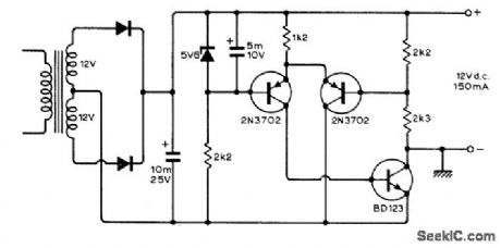
Three-transistor feedback circuit gives low-cost voltage stabilizer in which ripple is low and regulated output is very little less than unstabilized input voltage.-R. H. Pearson, Novel 5-Watt Class A Amplifier Uses Three-Transistor Feedback Circuit, Wireless World, March 1974, p 18. (View)
View full Circuit Diagram | Comments | Reading(1215)
_5_V_WITH_UNREGULATED__15_V
Published:2009/7/16 21:34:00 Author:Jessie
Developed for use with audio decoder that converts BCD output of digital display to audio tones that can be recognized by blind radio operator or experimenter.-D. R. Pacholok, Digital to Audio De-coder, 73 Magazine, Oct. 1977, p 178-180. (View)
View full Circuit Diagram | Comments | Reading(663)
ONE_CELL_CONVERTER
Published:2009/7/16 21:33:00 Author:Jessie
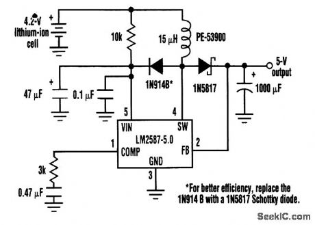
The regulator generates a 5-V output from a single lithium-ion cell. Initially, the lithium-ion cell is at 4.2 V, which is greater than the 3.75-V undervoltage-lockout (UVL) limit of the LM2587 Simple Switcher. Once it starts up, the boost circuit will continue to regulate-even when the battery voltage drops lower than the UVL limit. The level that the input voltage can drop to depends on the maximum load current desired. Of course, the source can be any type of battery-three alkaline, four NiCd, or even two lithium batteries. When power is applied to the circuit, the 10-kΩ resistor charges up the 47-μF input capacitor and supplies the startup current to the LM2587. After startup, the LM2587 input and the input capacitor draw current frorrt the switch node through the 1N914B boot-strap diode. When that happens, the IC input pin gets charged up to the output voltage minus a diode drop. In the circuit, with a 5-V output, the IC input voltage is 4.5 V after startup. It stays at 4.5 V-even when the input voltage drops to below 3.75 V. The input voltage can drop to 1.25 V when the regulator is supplying 250 mA. At 2.4 V, the regulator is 84 percent efficient if the 1N914B bootstrap diode is replaced with a 1N5817 Schottky diode. (View)
View full Circuit Diagram | Comments | Reading(2210)
3_IN_1_TEST_SET_LOGIC_PROBE_SIGNAL_TRACER_AND_INJECTOR
Published:2009/7/16 21:31:00 Author:Jessie
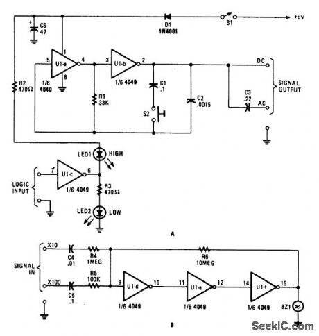
This circuit for a test set contains a signal injector (U1A/U1B) and associated components, a logic probe (U1C) and an audio amplifier. S1 selects either 10-kHz or 100-Hz output. U1D, U1E, and U1F form an audio amplifier that drives a piezo sounder element without an internal driver so that it functions as a piezoelectric speaker.
(View)
View full Circuit Diagram | Comments | Reading(1557)
LT1580_CIRCUIT
Published:2009/7/16 21:30:00 Author:Jessie

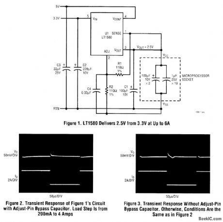
Figure 1 shows a circuit designed to deliver 2.5 V from a 3.3-V source with 5 V available for the control voltage. Figure 2 shows the response to a load step of 200 mA to 4.0 A. The circuit is configured with a 0.33-μF ADJUST-pin bypass capacitor. The performance without this capacitor is shown in Fig. 3. The difference in performance is the reason for providing the ADJUST pin on the fixed-voltage devices. A substantial savings in expensive output decoupling capacitance can be realized by adding a small ceramic capacitor at this pin. (View)
View full Circuit Diagram | Comments | Reading(746)
PROJECTION_LAMP_VOLTAGE_REGULATOR
Published:2009/7/12 22:30:00 Author:May
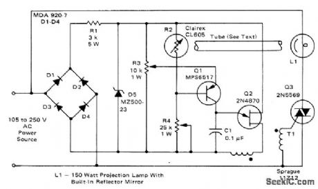
Circuit will regulate RMS output voltage across lamp to 100 V ±2% for input voltages between 105 and 250 VAC. Light output of 150-W projection lamp is sensed indirectly for use as feedback to firing circuit Q1-Q2 that controls conduction angle of triac Q3. Light pipe, painted black, is used to pick up red glow from back of reflectorinside lamp, which has relatively large mass and hence has relatively no 60-Hz modulation.- Circuit Applications for the Triac, Motorola, Phoenix, AZ, 1971, AN-466, p 12. (View)
View full Circuit Diagram | Comments | Reading(1570)
TRANSFORMERLESS±12V_AT_15_mA
Published:2009/7/12 22:29:00 Author:May
Develaped to ρrovide bias voltage for six 741 opamps.Circuit connects ditectly across 120-V 60-Hz AC line.Article gives design procedure to meet performance requirements. For values shown, ripple is 1.1 V. Diode types are not critical.-C.Venditti, Build this Transformerless Low-Volt-age Supply, EDN Magazine, Feb. 5, 1977, p 102. (View)
View full Circuit Diagram | Comments | Reading(864)
POLARITY_PROTECTION_RELAY
Published:2009/7/16 21:28:00 Author:Jessie
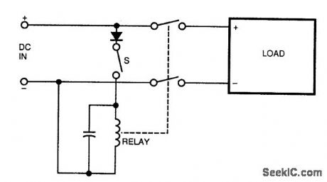
A diode prevents the relay from applying power polarity is reversed. (View)
View full Circuit Diagram | Comments | Reading(729)
SYMBOL_GENERATOR
Published:2009/7/16 21:27:00 Author:Jessie
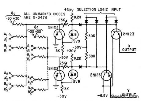
Combines sine and cosine waves of ten harmonic generators to produce X and Y waveforms for alphanumeric character generator.-K. E. Perry and E. J. Aho Radar-Computer Traces Alphanumeric Characters, Electronics, 34:26, p 75-79. (View)
View full Circuit Diagram | Comments | Reading(874)
CHARACTER_GENERATOR
Published:2009/7/16 21:26:00 Author:Jessie
Pulsed oscillator, used in producing alphanumeric display characters from combinations of circles, half-circles, and ellipses, is transient-free. Sinusoidal oscillator Q2 starts with full amplitude and stops in less than one cycle.-A. E. Popodi, Reliable Repertoire Of Display Circuits, Electronics, 38:2, p 60-66. (View)
View full Circuit Diagram | Comments | Reading(814)
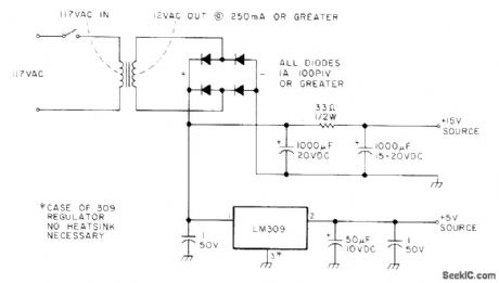
_5_V_AT_200_mA_OR_7_20_V_AT_100_mA
Published:2009/7/16 21:26:00 Author:Jessie
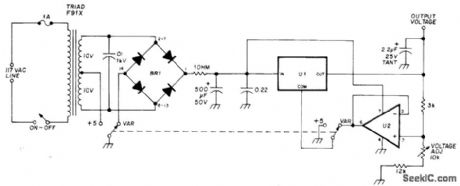
Uses National LM741 opamp as noninverting follower to sample output of voltage divider and drive common terminal of National LM340-05 three-terminal voltage regulator. Heatsink tab of regulator U1 must be connected to floating heatsink, BR1 is Adva bridge.-H. Olson, Second-Generation IC Voltage Regulators, Ham Radio, March 1977, p 31-37. (View)
View full Circuit Diagram | Comments | Reading(743)
TUBE_AMPLIFIER_ISOLATES_HIGH_VOLTAGES
Published:2009/7/16 21:26:00 Author:Jessie
This amplifier can transfer dc-to 5-MHz signals across a potential difference of 25000 V. This circuit can be used in CRT displays, high-voltage applications, etc. Notice that the tube must be shielded because the tube will generate X-rays. Typically, about 0.1 -thick sheet metal would be used. (View)
View full Circuit Diagram | Comments | Reading(1020)
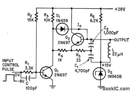
UNBLANKING_PULSE_GENERATOR
Published:2009/7/16 21:25:00 Author:Jessie
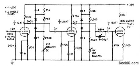
Unblanking signal is produced by repeated amplification and clipping of 500-cps signal from antenna synchro driver. Square-wave output is applied to control grid of display cut. Balancing controls are adjusted so unblanking strobe line starts from confer.-R. T.Wolfram, Improved Communications Using Groundscatter Propagation, Electronics, 33:44, p 74-78. (View)
View full Circuit Diagram | Comments | Reading(878)
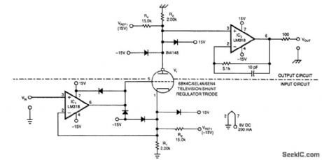
POWER_SUPPLY_MONITOR_MEMORY_PROTECTOR
Published:2009/7/16 21:25:00 Author:Jessie
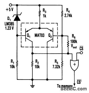
This circuit detects low-voltage supply conditions, down to 0.6 V. D1 sets the trip point of the circuit. The circuit is useful to protect memory circuits from accidental writes in the event of power-supply lowvoltage conditions, which cause other circuits to turn off, etc. Response time is about 700 ns. R6 provides some hysteresis to ensure clean transitions. (View)
View full Circuit Diagram | Comments | Reading(677)
_15_V_AND__6_V_TRANSFORM_ERLESS
Published:2009/7/16 21:25:00 Author:Jessie
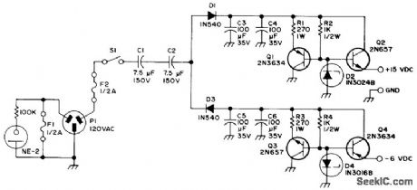
Transistorized regulator provides good voltage regulation with low ripple. Second ground prong is connected through fuse to grounded center conductor of AC line to guard against faulty AC wiring. If wiring is reversed, fuse will disable power supply and neon fault indicator will come on. At currents up to 55mA, -6 V output had 0.1-V ripple and +15 V output had 0.05-V ripple. - D. Kochen, Transformerless Power Supplies, 73 Magazine, Sept.1971, p 14-17. (View)
View full Circuit Diagram | Comments | Reading(707)
5_AND_15_V_DUAL_POLARITY_SUPPLY
Published:2009/7/16 22:29:00 Author:Jessie
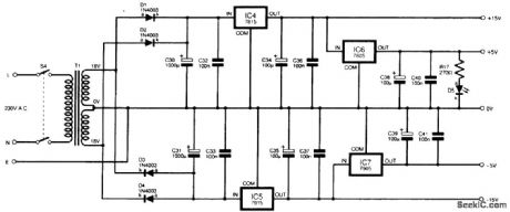
This supply will provide 5- and 15-V positive and negative voltages. It was used to power a MAX038 function generator, but it has other applications as well. (View)
View full Circuit Diagram | Comments | Reading(1167)
| Pages:88/291 At 2081828384858687888990919293949596979899100Under 20 |
Circuit Categories
power supply circuit
Amplifier Circuit
Basic Circuit
LED and Light Circuit
Sensor Circuit
Signal Processing
Electrical Equipment Circuit
Control Circuit
Remote Control Circuit
A/D-D/A Converter Circuit
Audio Circuit
Measuring and Test Circuit
Communication Circuit
Computer-Related Circuit
555 Circuit
Automotive Circuit
Repairing Circuit