
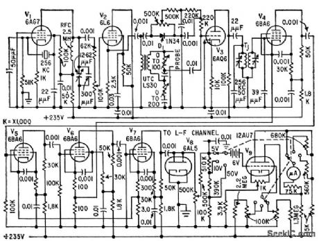
power supply circuit
Index 98
TUNED_OUTPUT_NE602_CIRCUITS
Published:2009/7/17 2:47:00 Author:Jessie
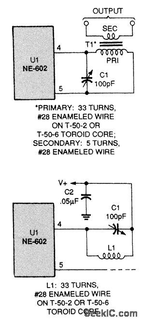
A tuned output like this one will reject all but the desired output signal.
Here is a single-ended tuned-output circuit. (View)
View full Circuit Diagram | Comments | Reading(750)
RECEIVER_IF_AMPLIFIER
Published:2009/7/17 2:46:00 Author:Jessie
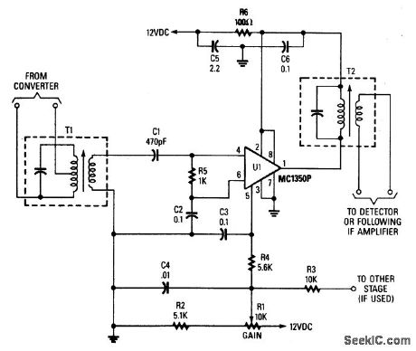
T1 is tuned to converter-output frequency U1 to provide 45-to-50-dB gain, depending on the design of T1 and T2. C2, C3, C4, CS, and C6 are bypass capacitors. R5 is a bias resistor. Gain is set by R1, which controls the voltage on pin 5 of U1. T1 and T2 should provide source and load impedance of 1-kΩ and 3-to 10 kΩ, respectively. R3 supplies dc bias to other stages, if required. (View)
View full Circuit Diagram | Comments | Reading(883)
CABLE_TERMINATION_FOR_VELOCIMETER
Published:2009/7/17 2:46:00 Author:Jessie
Amplifier restores leading edge of sinusoidal signal that has travailed through up to 35,000 feet of cable from deep-sea velocimeter. Frequency is then doubled by diodes, for ease of counting.-L. Dulberger, DeepOcean Velocimeter Aids Sonar Systems Design, Electronics, 34:22, p 41-43. (View)
View full Circuit Diagram | Comments | Reading(722)
UJT_PULSE_SHAPER
Published:2009/7/17 2:54:00 Author:Jessie
Use of inductance in ujt relaxation oscillator gives significant improvement in output pulse shape over that of conventional resistance-coupled circuit. Pulse width for various transistors is between 11 and 12 microsec, and rise and fall times are typically 0.3 microsec. With 47-ohm resistor in place of inductance, fall time would be 3 microsec.- Transistor Manual, Seventh Edition, General Electric Co., 1964, p 316. (View)
View full Circuit Diagram | Comments | Reading(2275)
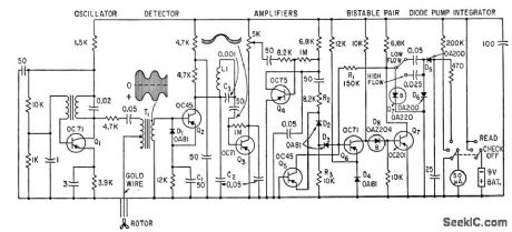
PORTABLE_FLOWMETER
Published:2009/7/17 2:54:00 Author:Jessie

Impedance between gold wire and blades of water-driven propeller changes a small amount as each blade passes within 0.1 mm of wire tip, giving amplitude modulation of 15-kc car rier generated by Q1. After demodulation,signal at propeller frequency is amplified, rectified, and integrated to drive velocity-indicating meter.-L. Molyneux and J. M.Edington, Portable Propeller Flowmeter Determines Water Velocity, Electronics, 34:25, p 60-62. (View)
View full Circuit Diagram | Comments | Reading(861)
TUNED_INPUT_CIRCUITS_FOR_NE6O2
Published:2009/7/17 2:54:00 Author:Jessie
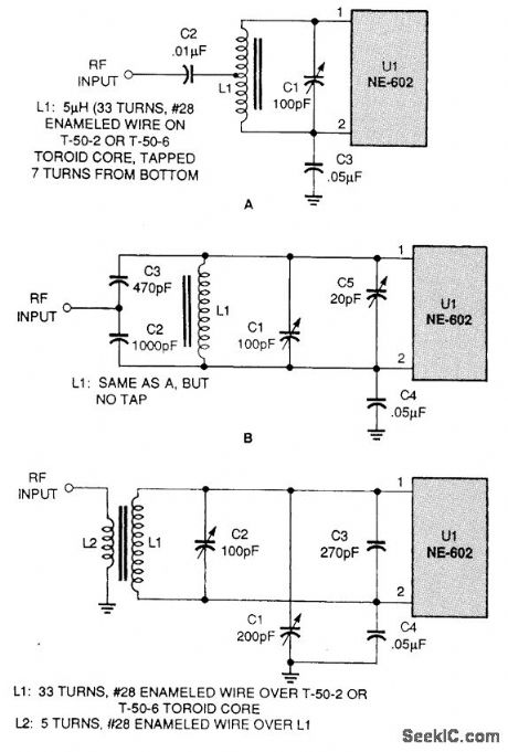
Here are three tuned input circuits. A tapped-inductor LC tuned circuit is shown in A and a flexible-tuned input circuit that can be used in a variety of situations is shown in C. (View)
View full Circuit Diagram | Comments | Reading(784)
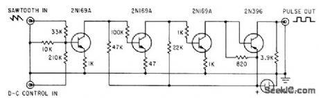
PULSE_LENGTH_CONTROLLER
Published:2009/7/17 2:53:00 Author:Jessie
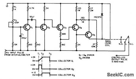
Reduces duration of intervalometer pulse from 400 millisec to 100 millisec without affecting intervalometer operation for other purposes Used to control airborne strip-chart camera.-J. S. Peddo, Low-Cost Pulse-Length Controller, EEE, 12:7, p 26. (View)
View full Circuit Diagram | Comments | Reading(866)
NE6O2_RF_INPUT_CONFIGURATIONS
Published:2009/7/17 2:53:00 Author:Jessie
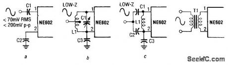
Here, (a) to (c) are for single-ended coupling, with (a) being for no impedance matching, (b) for tnductive matching, and (c) for capacitive matching. By contrast, (d) is a balanced input with reduced second harmonic. (View)
View full Circuit Diagram | Comments | Reading(650)
THICKNESS_GAGE_COMPENSATOR
Published:2009/7/17 2:52:00 Author:Jessie
High-frequency channel (256 kc) compensates for variation in probe-to-specimen spacing in eddy-current thickness gage for measuring cladding on reactor fuel elements.-W. J.McGonnagle, C. J. Renken, and R. G. Myers, Improved Nondestructive Testing by Eddy-Currents, Electronics, 32:35, p 42-43.
(View)
View full Circuit Diagram | Comments | Reading(763)
BROADBAND_NE602_SINGLE_ENDED_OUTPUT_CIRCUITS
Published:2009/7/17 2:51:00 Author:Jessie
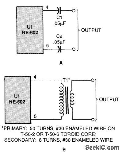
Here are two single-ended output circuits. A capacitor output is shown in A and a single-ended transformer output is shown in B. (View)
View full Circuit Diagram | Comments | Reading(709)
SINE_TO_SQUARE_WAVES
Published:2009/7/17 2:51:00 Author:Jessie
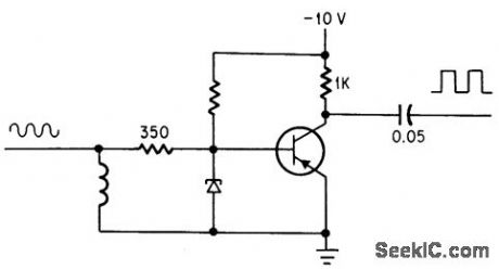
Japanese Esaki or tunnel diode acts like Schmitt trigger in converting sine-wave input signal to square-wave pulse train.-T. Kojima and M. Watanabe, When You're Second, You Try Harder, Electronics, 28:25, p 81-89. (View)
View full Circuit Diagram | Comments | Reading(1804)
500_KG_TO_1_MC_D_C_RESTORER
Published:2009/7/17 2:50:00 Author:Jessie
Modified damp circuit is used with 500-kc sine-wove input to provide complete restoration of reference potential for 1.Mc half-weave output.-H. Kundrat, Jr., High Frequency DC Restoration with Gain, EEE, lffi0, p 26-27. (View)
View full Circuit Diagram | Comments | Reading(737)
CARRIER_OPERATED_RELAY
Published:2009/7/17 2:50:00 Author:Jessie
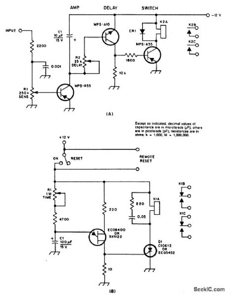
A shows a COR/CAS circuit for repeater use. CR1 is a silicon diode. K2 may be any relay with a 12-V coil (a long-life reed relay is best). R2 sets the length of time that K2 remains closed after the input voltage disappears(hang time). B shows atimer circuit. Values shown for R1 and C1 should provide timing up to four minutes or so. C1 should be a low-leakage capacitor; Q1 is a silicon-controled rectifier, ECG-5452 or equivalent. K1 may be any miniature relay with a 12-volt coil. The timer is reset when the supply voltage is momentarily interrupted. The switch must be in the RESET position for the remote reset to work. This circuit operates from the detector output of a receiver. A delay circuit is included so that the relay stays closed for a time period after the carrier output from the receiver disappears. (View)
View full Circuit Diagram | Comments | Reading(5444)
TRANSIENT_RESPONSE_OF_REGULATED_SUPPLlES
Published:2009/7/11 3:48:00 Author:May
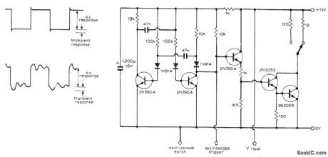
Developed for testing transient response of 12-V regulated power supply at loading of either 100 mA or 1 A,depending on switch position. Load resistors ean be changed for other voltages and currents. Transients generated by supply may be observed on AC-coupled oscilloscope. Good transient response will show only small leading-edge peaks, as in upper waveform. Any tendency of power supply toward instability degrades waveform much more, as in lower diagram. Circuit consists of multivibrator using series diodes in base circuits to protect transistors from excessive voltage swings in switching cycle. Square-wave output is used for oscilloscope trigger and fed to other three transistors that provide load for power supply under tesl.-H. Macdonald, Transient Response Testing, Wireless World, July 1973, p 338. (View)
View full Circuit Diagram | Comments | Reading(803)
Series_shunt_analog_switch_useful_in_applications_requiring_extremely_low_input_to_output_signal_feedthrough_
Published:2009/7/17 2:46:00 Author:Jessie
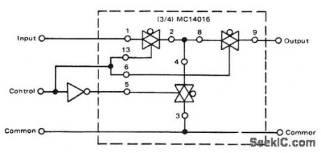
Series-shunt analog switch, useful in applications requiring extremely low input-to-output signal feedthrough (courtesy Motorola Semiconductor Products Inc.). (View)
View full Circuit Diagram | Comments | Reading(867)
SCS_PULSE_STRETCHER
Published:2009/7/17 2:45:00 Author:Jessie
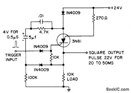
Stretch interval is determined by 5-mfd capacitor and 4.7K resistor.- Transistor Manual, Seventh Edition, General Edition Co, 1964, p 435. (View)
View full Circuit Diagram | Comments | Reading(668)
HF_TRANSCEIVER_MIXER
Published:2009/7/17 2:41:00 Author:Jessie
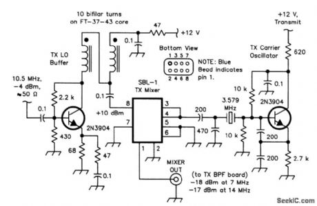
The transceiver mixer and carrier oscillator in the band-imaging (7- and 14-MHz) CW transceiver. Careful selection of drive levels, and use of a spectrally clean carrier oscillator, assure low spurious-signal content in the transmitter output. This transceiver mixer should prove useful in HF and VHF CW or SSB applications. A Mii-Circuits SBL1 low-cost mixer is used with a 3.579-MHz crystal oscillator that uses a low-cost TV color-burst crystal. By paying careful attention to drive leads, good performance and low spurious content can be obtained. (View)
View full Circuit Diagram | Comments | Reading(3807)
Diode_bridge_clamping_circuit_to_improve_A_D_convener_performance_
Published:2009/7/17 2:41:00 Author:Jessie
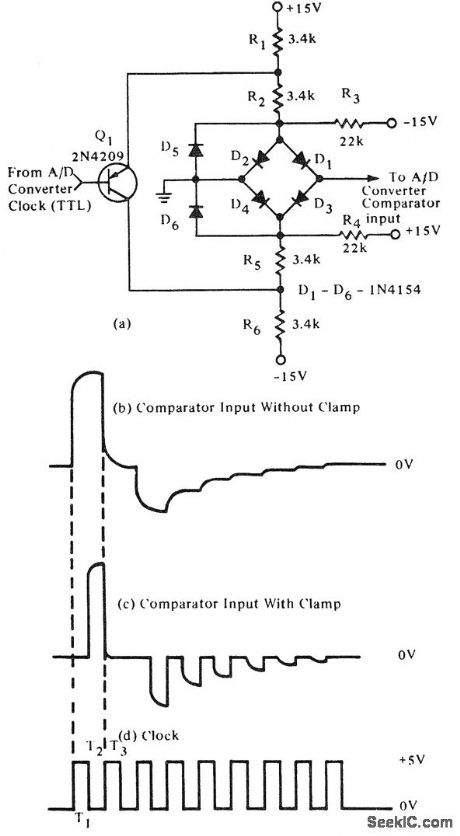
Diode-bridge clamping circuit to improve A/D convener performance (courtesy Burr-Brown Corporation). (View)
View full Circuit Diagram | Comments | Reading(804)
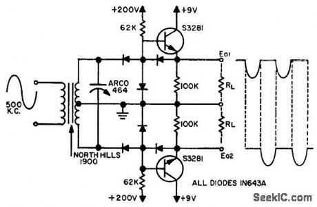
NE6O2_OUTPUT_CIRCUITS
Published:2009/7/17 2:40:00 Author:Jessie
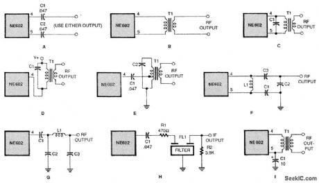
The various output circuits shown here demonstrate how to either pass all the frequencies from the NE602 or allow only the sum or difference frequencies through, depending on which circuit is used.
(View)
View full Circuit Diagram | Comments | Reading(799)
VARIOMETER_RADIO
Published:2009/7/17 2:39:00 Author:Jessie
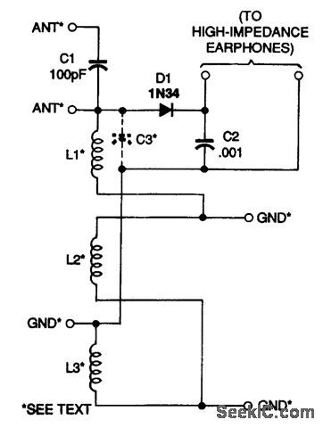
The schematic of the complete variometer radio is shown in the figure. An antenna can be connected to the radio through either of the two points labeled ANT: either directly to the circuit or through a 100-pF capacitor. The ground connection can be made at any of the points marked GND.There is a reason for the preceding options: By varying the antenna capacitance, the ground connection, and the position of the sliding coil, the entire AM broadcast band can be tuned. Depending on the antenna and ground connections, it might be necessary to add a small capacitor, C3, at the point indicated in the schematic. If so, experiment with values between 25 and 200 pF (separately or in parallel) to find which gives the best result. If you build the variometer using Fahnestock clips (as explained later), adding the capacitor(s) after the radio is built if the need arises should be easy. When a signal is selected by adjusting the antenna, ground connection, and position of L2, the signal is passed on to the diode-detector part of the circuit, composed of D1, which demodulates the signal. The signal then goes through bypass capacitor C2 to the earphones. Only high-impedance earphones should be used with the variometer. L1 and L3 are 86 turns of #22 wire on a 1.25-inch form, and L2 is 74 turns of #22 wire on a 1.75-inch form. (View)
View full Circuit Diagram | Comments | Reading(1145)
| Pages:98/291 At 2081828384858687888990919293949596979899100Under 20 |
Circuit Categories
power supply circuit
Amplifier Circuit
Basic Circuit
LED and Light Circuit
Sensor Circuit
Signal Processing
Electrical Equipment Circuit
Control Circuit
Remote Control Circuit
A/D-D/A Converter Circuit
Audio Circuit
Measuring and Test Circuit
Communication Circuit
Computer-Related Circuit
555 Circuit
Automotive Circuit
Repairing Circuit