
power supply circuit
Index 87
ALPHANUMERIC_CHARACTER_GENERATOR
Published:2009/7/16 21:55:00 Author:Jessie
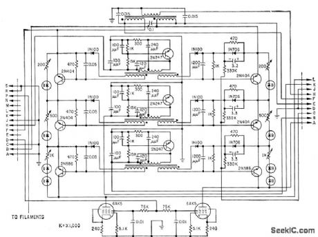
Used to Provide readout on cathode-ray display as output of digital computer. Horizon-tal decoding and deflection circuits are shown.240 Vertical circuitry is essentially identical.-E.D. Jones, Character Generator for Digital Computers,Electronics,33:7, p 117-120. (View)
View full Circuit Diagram | Comments | Reading(1089)
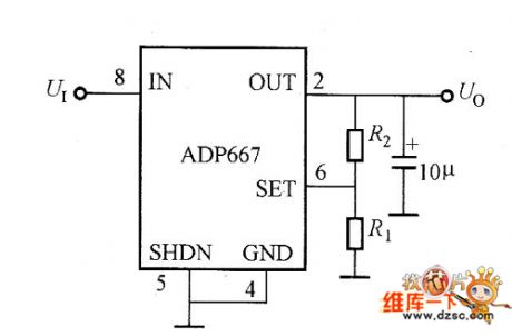
ADP667 adjustable output voltage circuit diagram
Published:2011/7/20 5:20:00 Author:nelly | Keyword: adjustable output voltage
View full Circuit Diagram | Comments | Reading(698)
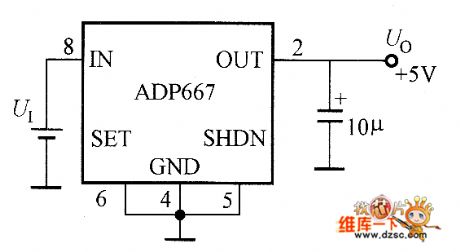
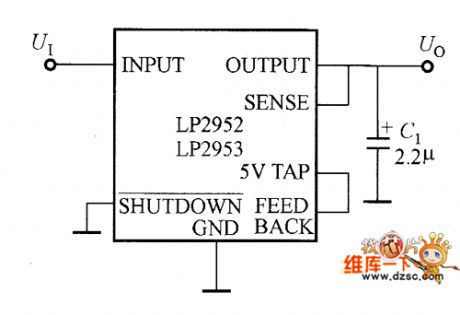
ADP667 5V fixed voltage output circuit diagram
Published:2011/7/20 5:21:00 Author:nelly | Keyword: fixed voltage output
View full Circuit Diagram | Comments | Reading(925)
5_V_AT_1_A
Published:2009/7/16 21:54:00 Author:Jessie
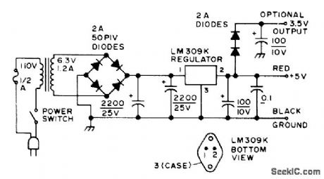
Can handle over 30 TTL ICs in frequency counter if LM309K regulator is mounted directly on aluminum heatsink. Case of regulator is grounded, so mica insulation is not needed. Provides excellent regulation with practically no output ripple and is short-circuit-proof. Circuit also shuts itself off if temperature gets too high. - P. A, Stark, A Simple 5 V Power Supply for Digital Experiments, 73 Magazine, Oct. 1974, p 43-44. (View)
View full Circuit Diagram | Comments | Reading(0)
5V fixed voltage output circuit diagram
Published:2011/7/20 5:23:00 Author:nelly | Keyword: 5V voltage output, fixed voltage output
View full Circuit Diagram | Comments | Reading(652)
±15_V_1
Published:2009/7/16 21:53:00 Author:Jessie
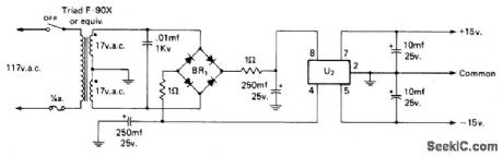
Developed for use in two-tone AF generator for testing SSB equipment. BR1 is Motorola HEP176 or MDA-920. U2 is Raytheon 4195DN.-H. Olson, A One-Chip, Two Tone Generator, CQ, April 1974, p 48-49. (View)
View full Circuit Diagram | Comments | Reading(745)
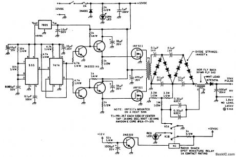
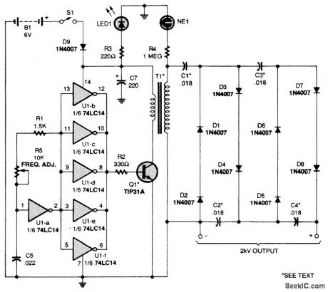
JACOBS_LADDER_HV_SUPPLY
Published:2009/7/16 21:51:00 Author:Jessie
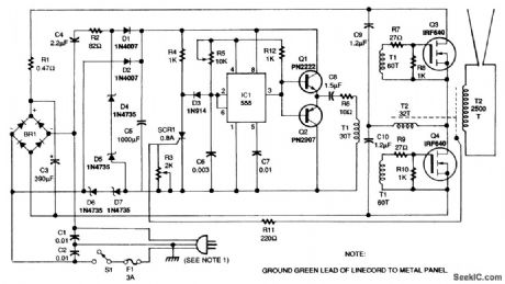
The operation of the Jacobs's Ladder depends on the current-limited power supply that delivers 12,000 V at 40 mA from the 120-Vac line. The full-wave bridge BR1 rectifies the 120-Vac line input, and resistor R1 limits the dc charging current of capacitor C3 to a safe value. The drive circuit power is obtained by dropping the 120-Vac line through capacitor C4 and current-limiting resistor R2. Capacitor C4 and resistor R2 present a complex impedance, so most of the ac line voltage is dropped across the reactance. The 555 timer IC is configured as a square-wave oscillator. The output frequency of its square waves is determined by the setting of trimmer potentiometer R5 and capacitor C6. The frequency is about 25 kHz for the values of R5 and C6 shown. Potentiometer R5 can be used to adjust the circuit's power output. Increasing the frequency reduces the circuit's output by increasing the inductive reactance of the transformer leakage inductance. The output of IC1 on output pin 3 appears at the bases of the current source, NPN transistor Q1, and sink, PNP transistor Q2. The emitters of this transistor pair are ac-coupled through capacitor C8 and resistor R6 to drive the primary of driver-isolation transformer T1. This drive prevents dc from flowing through the primary. Transformer T1 is wound on a high-permeability core with as few turns as possible to eliminate leakage inductance. The gate circuits of MOSFETs Q3 and Q4 contain 27-Ω resistors (R7 and R9) to slow their switching times. This eliminates possible parasitic oscillations that could occur if the MOSFETs were switched at their speed limit. The primary of output transformer T2 contains 32 turns, but its secondary contains 2500 turns. The ratio of these turns is approximately 1 to 78. When this is multiplied by the rectified line voltage of 160 Vdc, an output of about 12,000 peak volts is obtained across the secondary. This 12,000-V output is the peak open-circuit voltage of the system, and it produces a short-circuit current of approximately 40 mA. This current is limited by the leakage inductance caused by the loose magnetic coupling between the primary and secondary circuits of transformer T2. (View)
View full Circuit Diagram | Comments | Reading(3576)
PHOTOMULTIPLIER_TUBE_SUPPLY
Published:2009/7/16 21:49:00 Author:Jessie
This circuit is quite efficient, drawing virtually no current when the load is a photomultiplier (PM) used as a scintillation detector. Be sure that the voltage-divider resistors on the PM tube are very high to conserve power-the higher the better. If the high-voltage circuit uses a diode voltage-multiplier chain, then connect the chain to the transformer, just as the three-diode doubler is connected. Lower the regulated voltage by removing one of the neons or by selecting an appropriate zener. If a higher voltage is needed, simply extend the diode multiplier. (View)
View full Circuit Diagram | Comments | Reading(2487)
HELIUM_NEON_LASER_POWER_SUPPLY_WITH_HV_PULSE_IGNITION
Published:2009/7/16 21:48:00 Author:Jessie
The helium-neon laser requires two voltages: a voltage in the range of 10 kV that starts the laser and then turns off once the discharge begins, and a lower-voltage power supply to sustain the dis-charge. The circuit diagram illustrates one method of generating the laser ignition voltage. A fraction of the main supply voltage is used to charge up a capacitor. When triggered, it is discharged through a high-voltage ignition transformer in series with the main power supply output. When the supply is first turned on, a delay circuit allows the main supply to stabilize at full voltage and charge up the capacitor. A nonlatching relay operates to discharge the capacitor into the ignition coil on a one-shot basis after the timing delay. The HV diode in series with the ignition coil and the capacitor across the supply rectifies the damped oscillatory waveform out of the ignition coil, producing a single positive pulse across the laser tube to ionize the gas in the laser. Once the laser is ignited by the HV pulse, the main power supply maintains the discharge. (View)
View full Circuit Diagram | Comments | Reading(3710)
FINE_POSITIONING_CHARACTER
Published:2009/7/16 21:47:00 Author:Jessie
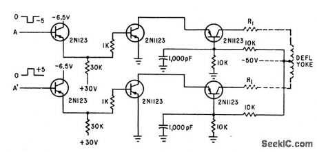
GENERATOR SWTICH-Pairs of deflection Switches operating push-pull into defection yoke act with 16-point coarse positioning system to give 4,096 positions, generated in binary fashion.-K.E Perry and E.J. Aho, Radar-Computer Display fracas Alphanumeric Characle,Electronics,34:26,p 75-79. (View)
View full Circuit Diagram | Comments | Reading(926)
REGULATOR_FOR_700_V_LOW_CURRENT_SUPPLY
Published:2009/7/16 21:45:00 Author:Jessie
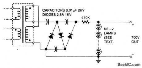
If you need a regulated output, change the voltage doubler to a tripler, and use neon lamps as a regulator. The number of lamps you will need will depend on the characteristics of the lamps used, and will have to be found by experimentation. Each lamp has approximately a 55- to 70-V the break-down voltage. The lamps should be shielded from light (or painted black) because light can influence the breakdown voltage. (View)
View full Circuit Diagram | Comments | Reading(761)
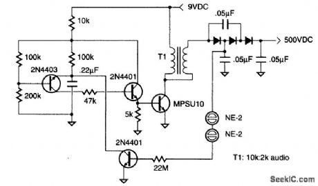
GEIGER_COUNTER_700_V_LOW_CURRENT_SUPPLY
Published:2009/7/16 21:45:00 Author:Jessie
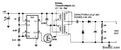
This 700-V, 0.25-mA power supply converts a +9-Vdc input to 10-kHz ac, then uses the setup transformer and the voltage-doubler circuit to produce the required output. (View)
View full Circuit Diagram | Comments | Reading(1539)
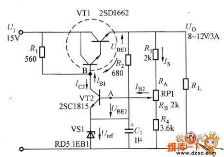
Regulated power supply circuit diagram with adjustable transistor output voltage
Published:2011/7/20 5:10:00 Author:nelly | Keyword: Regulated power supply, transistor, output voltage
View full Circuit Diagram | Comments | Reading(2103)
BASIC_CHARGE_PUMP_CIRCUIT
Published:2009/7/16 21:44:00 Author:Jessie
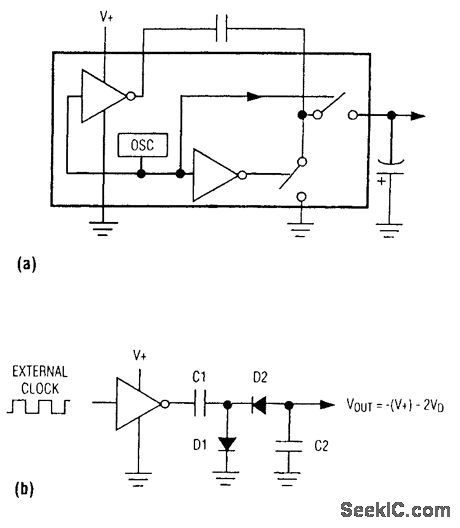
A basic charge pump provides voltage doubling or inversion. It can be implemented with on-chip switches (a) or discrete diodes (b). (View)
View full Circuit Diagram | Comments | Reading(1103)
UNIVERSAL_TEST_PROBE
Published:2009/7/16 21:42:00 Author:Jessie
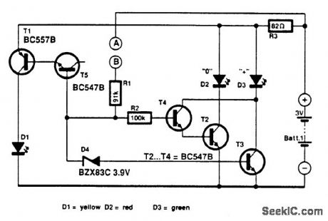
The compact test prbbe provides rapid measurement of voltage levels at digital gates, fuses, diodes, batteries, and others. It does not provide absolute values, but rather it provides a good indication of correct operation or otherwise.
Measurements are carried out with pins A and B. If the potential difference between A (the reference pin) and B is 1.9 to 2.0 V, D2 will light. If the voltage at B is ≤ 1.4 V higher than that at A, D3 will light. Finally, if the potential at B is a 11 V, with respect to that at A, D1 will light.
Transistor T5 is used as a zener diode. The probe allows the measurement of alternating voltage. The maximum input voltage is highly dependent on the dissipation allowed in R1. For example, when this resis-tor is a 0.5-W type, the input voltage can be as high as 200 Vrms.
The current drawn by the circuit depends on the number of lighting LEDs: it is not more than 10 mA at a supply voltage of 3 V. In quiescent operation, the current is so low (about 5μA) that an on/off switch is not necessary. (View)
View full Circuit Diagram | Comments | Reading(875)
HELIUM_NEON_LASER_SUPPLY_WITH_HV_MULTIPLIER_IGNITION
Published:2009/7/16 21:40:00 Author:Jessie
This figure illustrates a way in which a momentary 10-kV voltage pulse can be generated to initiate the plasma discharge across the laser tube. A Diode voltage-multiplier circuit is connected in series with the main supply and obtains its input power across one of the voltage-multiplier diodes in the main supply. The voltage across this diode is typically 1.8 kV p-p With a ten-section multiplier, the output voltage is approximately 9 kV in series with a 1.8-kV sustaining supply. The capacitors value of the capacitors in the multiplier chain is much smatter than that of the capacitors for the main supply. When the power supply is first turned on, the capacitors in the voltage multiplier charge up to the ignition voltage. As the plasma forms, the laser tube draws more current and the multiplier capacitors cannot maintain their charge. As a result, the voltage immediately drops to that of the main sustaining supply, with all the diodes in the multiplier chain forward-biased. In this manner, an HV pulse is generated to ionize the gases. (View)
View full Circuit Diagram | Comments | Reading(4775)
LOGIC_TESTER
Published:2009/7/16 21:39:00 Author:Jessie
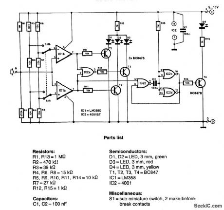
The input consists of two comparators that operate with different reference voltages supplied by separate potential dividers. Divider R3/R4/R5 provides a voltage of about 40% of the supply voltage, UCC, to pin 6 of IC1B and one of about 16% of UCC to pin 3 of UC1A. When UCC = 5 V, these voltages are exactly the thresholds (0.8 and 2.0 V) of the TTL comparators.
Similarly, divider R6/R7/R8 provides voltages of 23% of UCC and 73% of UCC to pin 3 of IC1A and pin 6 of IC1B respectively; these levels correspond to the standard threshold for CMOS comparators.
The voltage to be measured Ua, is applied to pin 5 of IC1B and pin 2 of IC1A and compared with the respective reference. The output of comparator IC1B goes high when Ua, exceeds the reference, whereas the output of IC1A goes high when Ua lies below the voltage at pin 3.
The comparators are followed by driver stages, T1 and T2, for the LED display (D1 for high and D2 for low ) and also NOR gate IC2A that switches on T3 when the output of both comparators is low, that is, when it is undefined. This state is indicated by D3.
The remaining three gates in IC2 form a monostable. During quiescent operation, UCC is present at the input of inverter IC2C. The output of the inverter is then low, T4 is off and D4 is out. Pin 4 of IC2B is also high, but this state changes when a pulse arrives at pin 5. The output of IC2B then goes low, C2 discharges, the inverter toggles, T4 is switched on, and D4 lights. This state is unstable, however, because C2 recharges via R13, Although the pulse at pin 5 might be very short, the time constant R13/C2 lengthens it to about 100 ms.
The supply voltage can lie between 5 and 15 V. At 5 V, the circuit draws a current of about 15 mA. The input impedance of the tester is of the order of 330 kΩ. (View)
View full Circuit Diagram | Comments | Reading(1122)
POPULAR_VOLTAGES_SUPPLY
Published:2009/7/16 21:38:00 Author:Jessie
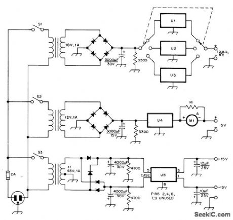
Provides most common fixed voltages required for transistor and IC projects. Eliminates cost and nuisance of replacing batteries. Provides t15 V at 100mA, +5 V at 1 A, and choice of +6.0, +8.2, and +12.0 V at 1 A. Separate grounds (not chassis grounds) permit connecting supplies in series to get combination voltages. Rectifier diodes are 100 PIY at 1 A. Use meter and shunt to give full scale at 1 A; for 150-mA meter, use 0.08 ohm for R1 (six 0.5-ohm resistors in parallel). U1 is LM340K-12, U2 is LM340K-8, U3 is LM340K-6, U4 is LM340K-5, and U5 is 4195.-C.J. Appel, A Combination Fixed-Voltage Supply, QST, Nov. 1977, p 36-37. (View)
View full Circuit Diagram | Comments | Reading(845)
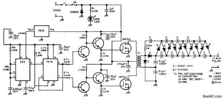
HIGH_VOLTAGE_POWER_SUPPLY
Published:2009/7/16 21:38:00 Author:Jessie
This circuit uses a transformer to generate a high-voltage output (up to 20,000 V) from just four C cells. T1 can be a 50 to 100:1 turns ratio unit or can be made from a flyback transformer from a junked B/W TV. (View)
View full Circuit Diagram | Comments | Reading(0)
LASER_RECEIVER_PHOTOMULTIPLIER_TUBE_SUPPLY
Published:2009/7/16 21:37:00 Author:Jessie
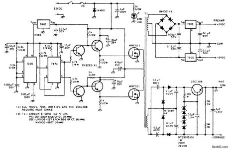
The figure shows the circuit diagram of a regulated 1000-Vdc power supply driven from a 12-Vdc source. A low-voltage secondary regulated power source supplying power to the PMT video pre-amplifier is included. Again, follow the caution regarding PMT power supplies. All precautions must be observed when working with the PMT high-voltage supply. (View)
View full Circuit Diagram | Comments | Reading(2655)
| Pages:87/291 At 2081828384858687888990919293949596979899100Under 20 |
Circuit Categories
power supply circuit
Amplifier Circuit
Basic Circuit
LED and Light Circuit
Sensor Circuit
Signal Processing
Electrical Equipment Circuit
Control Circuit
Remote Control Circuit
A/D-D/A Converter Circuit
Audio Circuit
Measuring and Test Circuit
Communication Circuit
Computer-Related Circuit
555 Circuit
Automotive Circuit
Repairing Circuit