
power supply circuit
Index 81
POWER_BUFFER_BOOSTS_REFERENCE_CURRENT
Published:2009/7/16 21:24:00 Author:Jessie
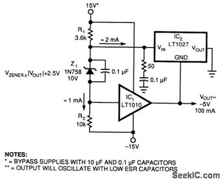
A method of boosting the output current of a reference and also protecting against overloads is shown in Fig. 66-5. IC1 acts as a power buffer. The LT1027 forces the output of VOUT and ground to be 5 V. The RC damper (50Ω and 0.1 μF) provides loop stability. The output might oscillate if low ESR capacitors are connected to it, so use aluminum electrolytic or tantalum capacitors instead of ceramic or mylar. (View)
View full Circuit Diagram | Comments | Reading(929)
EFFICIENT_REGULATED_STEP_UP_CONVERTER
Published:2009/7/16 21:24:00 Author:Jessie
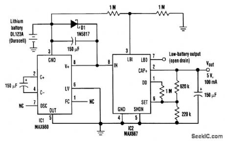
Two eight-pin ICs form a regulator circuit that can convert a lithium battery's 3-V output to 5 V and deliver load currents as high as 100 mA. It operates without inductors or transformers, and draws only 200 μA of quiescent current. At Vin = 3 V, it offers 81-percent efficiency with a 100-mA load and 84 percent with a 20-mA load. Efficiency will increase as Vin falls. For example, at Vin = 2.7 V (the cell's loaded output for most of its operating life), efficiency for a 40-mA load current is 90 percent. Voltage from the lithium battery (a 2/3-A size Duracell DS123A) is doubled by the high-current charge pump (IC1). The Schottky diode (D1) is included to assure startup in this configuration.D1 won't affect efficiency because it doesn't conduct load current during normal operation. IC2 is a linear regulator with a dropout voltage of only 40 mV at Iload 40 mA. This load, allowed to drain the battery until Vout = 4.5 V, yields a battery life of 16 hours. Reducing the load to 20 mA extends the battery life to 36 hours. (View)
View full Circuit Diagram | Comments | Reading(948)
CONSTANT_CURRENT_TEST_LOAD
Published:2009/7/16 21:23:00 Author:Jessie

This circuit will supply a constant load of 500 mA to 1.5A. R4 controls the current while R3 provides fine adjustment. (View)
View full Circuit Diagram | Comments | Reading(1348)
Z_AXIS_MODULATION
Published:2009/7/16 21:22:00 Author:Jessie
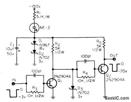
Pulse amplifier allows crt beam-intensity modulation from 3.v logic levels.Requires only single -150 v supply. Intended as modification for Tektronix oscilloscope.-J. H.Cormack, Pulse Amplifier for Beam Intensity Modulation, EEE, 14:1, p 63. (View)
View full Circuit Diagram | Comments | Reading(915)
BACKUP_SUPPLY_ACTIVATES_BY_DROP_IN_MAIN_SUPPIJY
Published:2009/7/16 21:22:00 Author:Jessie
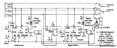
A supply monitor using two TL7702A chips monitors the ±15-V supplies and activates the backup supply in case of a voltage drop. Although the chips are intended for use as reset controllers in microprocessor systems, they work well in this application. (View)
View full Circuit Diagram | Comments | Reading(846)
±6_AND_±15_V
Published:2009/7/16 21:22:00 Author:Jessie
Developed for use with function generator. Mount regulators on heatsinks insulated from chassis by mica wafers. Article covers construction and adjustment to give exactly desired outputs.-H. Olson, Build This Amazing Function Generator, 73 Magazine, Aug. 1975, p 121-124. (View)
View full Circuit Diagram | Comments | Reading(921)
PWM_TELEMETRY
Published:2009/7/16 21:21:00 Author:Jessie
Width or height of input pulse determines whether trigger Q1-Q2 will be on long enough for C to charge to voltage that will make trigger Q3-Q4 produce output pulse.-R. G. Ferrie, One Discriminator Senses Pulse Width and Height, Electronics, 38:8, p 90-91.
(View)
View full Circuit Diagram | Comments | Reading(839)
LIGHT_PEN_PREAMP
Published:2009/7/16 21:21:00 Author:Jessie
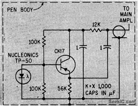
Raises signed level of germanium photodiode before it is fed through coax to main amplifier. Special decoupling in collector circuit allows power and signal to be supplied simultaneously over single coaxial cable.-B. M. Gurley and C. E. Woodward, Light-Pen Links Computer to Operator, Electronics, 32:47, p 85-87. (View)
View full Circuit Diagram | Comments | Reading(938)
CIRCUIT_BREAKER_TRIPPER
Published:2009/7/16 21:21:00 Author:Jessie
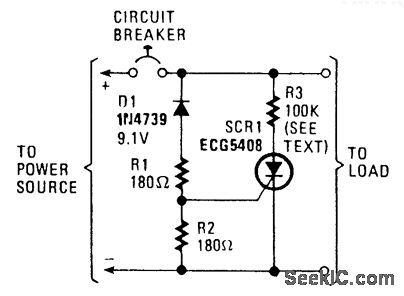
This tripper is designed to protect against overvoltages. D1 conducts over 9.1 V and triggers SCR1. R3 is chosen to draw enough current to trip the breaker. (View)
View full Circuit Diagram | Comments | Reading(1279)
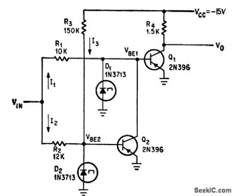
VOLTAGE_REGULATOR_SINKS_AND_SOURCES
Published:2009/7/16 21:21:00 Author:Jessie
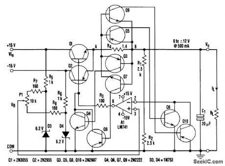
It is possible to build a circuit that provides a variable output from -12 to +12 V (passing smoothly through 0 V) that can source or sink at any voltage. The basic regulator consists of an op amp (A1), series pass transistors Q1 and Q2, a reference voltage from Pl, and a voltage divider (R1 and R2). The rest of the elements provide short-circuit protection for the regulator. The reference voltage is generated by zener diodes D3 and D4. With a 10-turn potentiometer (P1), the reference voltage (VR) for the of amp can be varied from -6 to +6 V. The output voltage is given by VO = VR (1 + R1/R2) Because R1 = R2, the output can be varied from 0 to ±12 V. When VO is positive and the regulator is sourcing current (IL positive), the base of Q1 is at VO+ 0.7m and Q1 is conducting. When VO is positive and RL is terminated in a supply voltage higher than VO, the regulator is forced to sink current (IL negative). At this time, Q2 conducts and sinks the current, and A1 maintains the base of Q2 at VO- 0.7. Similar arguments apply when the output voltage is negative. C1, a nonpolarized electrolytic capacitor, prevents oscillations. R4 is a current-sensing resistor for short-circuit protection and limits the output current to 55 mA. For a positive VO, if IL is positive (sourcing) and reaches 500 mA, the voltage drop VAB across R4 approaches 0.7 V and forward-biases the E-B junction of Q3. Q3 conducts and drives the base of Q4. Because Q4 goes into saturation as a result of the drop across R3, it clamps the base voltage of Q1 to ground and the output voltage drops, limiting the current in Q1 to 500 mA. Similarly, under a positive VO, if IL is negative (sinking) and reaches 500 mA, VAB across R4 approaches -0.7 V and forward-biases the E-B junction of Q5. Q5 drives Q6 into saturation, and the inverting input of the op amp is clamped to ground. Because the noninverting input is held at VR (which is still positive), the output starts climbing toward +15 V. This prevents Q2 from sinking more current than 500 mA. Under a negative VO, with IL negative, Q7 and Q8 provide short-circuit protection, With VO negative and positive, Q9 and Q10 provide short-circuit protection. (View)
View full Circuit Diagram | Comments | Reading(870)
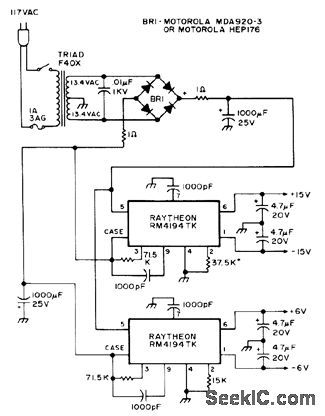
±15_V
Published:2009/7/16 21:20:00 Author:Jessie
Provides positive and negative supply voltages required by some opamps. Supply is short-circuit-proof and protects itself against overloads. –I. Math, Math’s Notes, CQ, Jan. 1974, p 68-69. (View)
View full Circuit Diagram | Comments | Reading(887)
ISOLATED_VOLTAGE_SENSOR
Published:2009/7/16 21:20:00 Author:Jessie
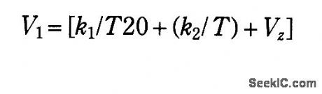
A simple voltage-controlled oscillator (VCO), coupled to your instrumentation by an optoisolator, allows you to measure high voltages. The component values suit a 0- to 600-V input range (power dissipation in R1 and R2 set a limit on the input-voltage range). The circuit's linearity is not an issue, because you can linearize its output in software.
The input voltage (V1), charges capacitor C1 until zener diode D1 conducts. Then, the zener diode triggers an avalanche circuit that discharges C1 into optocoupler Q1. After C1 discharges, the charging cycle repeats. C1 also averages the sensed-voltage level, which thereby provides noise immunity.
The optocoupler's output is a pulse train whose frequency increases with increasing input voltage. To develop a linearizing equation for the circuit, measure its output at two convenient, widely spaced input voltages. Then plug the resulting periods into this second-order polynomial approximation and solve the two simultaneous equations for the two constants, k1 and k2:
Vz is the zener voltage of D1. (View)
View full Circuit Diagram | Comments | Reading(1876)
VOLTAGE_DISCRIMINATOR
Published:2009/7/16 21:19:00 Author:Jessie
Output changes sharply when input signal rises above preset threshold such as -10 v, with circuit returning to initial state when input reaches still higher threshold such as -11 v. Width of resulting output pulse can be changed by varying R1, R2, or R3.-C. D. Todd, Sharp Discrimination of Voltage Differences, Electronics, 38:19, p 97-98.
(View)
View full Circuit Diagram | Comments | Reading(948)
7_AL_25_V_SUPPLY
Published:2009/7/16 21:18:00 Author:Jessie
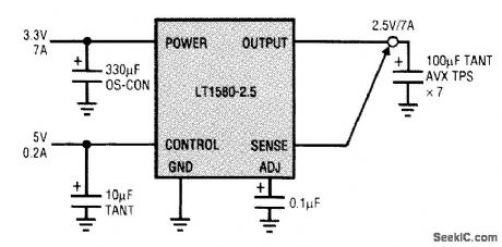
The latest microprocessors use low-voltage processes that allow the clock frequencies to increase dramatically. Increased clock frequencies result in higher core-supply currents. Several next-generation microprocessors will use a 2.5-V supply voltage and require greater than 5-A supply current. The LT1580-2.5 in the circuit shown has the lowest dropout of any 7-A linear regulator, only 0.6 V typical. This allows conversion from a standard 3.3-V main supply down to 2.5 V. In order to achieve this low dropout performance, a second low-current control supply 1.3V greater than the 2.5 V output is needed. A system 5-V supply conveniently provides this voltage, and only 200 mA is required from the control supply. The LT1580-2.5 also has fast transient response to load-current steps, minimizing required bulk output capacitance. An internal reference voltage with ±0.5 percent initial tolerance and Kelvin sense input make the output regulation very tight. (View)
View full Circuit Diagram | Comments | Reading(772)
0_TO_50_V_VARIABLE_REGULATOR
Published:2009/7/16 21:17:00 Author:Jessie
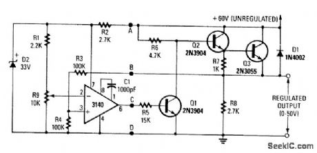
A CA3140 op amp compares the regulator output to a reference voltage, depending on the setting of R9. The output voltage will be nominally twice the voltage between the plus input of the CA3140 and ground. R1 and R9 allow 0 to 50 V. (View)
View full Circuit Diagram | Comments | Reading(1223)
RASTER_TIMING_GENERAIOR
Published:2009/7/16 21:17:00 Author:Jessie
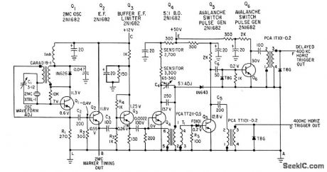
Crystal oscillator (2 Mc) triggers blocking oscillator Q4 that counts down by 5 to produce 400-kc timing pulses for test oscilloscope using tv-type scanning.-R. P. Rufer and W. A Karotski, Use Raster Oscilloscopes for Easter Time Measurement,Electronics,35:52,p 38-42. (View)
View full Circuit Diagram | Comments | Reading(767)
PULSE_AMPLITUDE_DISCRIMINATOR
Published:2009/7/16 21:17:00 Author:Jessie
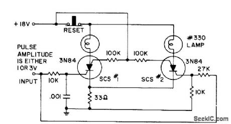
Input of1 v triggers SCS1 but not SCS 2. Input of 3 v is delayed in reaching SCS1 by R-C info. grating network and therefore triggers SCS2, which raises common-emitter voltage lo prevent SCS1 from triggering. - Transistor Monual, Seventh Edition, General Electric Co., 1964, p 433. (View)
View full Circuit Diagram | Comments | Reading(1466)
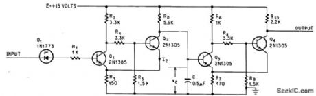
SIMPLE_DARLINGTON_REGULATOR
Published:2009/7/16 21:15:00 Author:Jessie
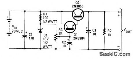
A Darlington pair is used as an emitter-follower that produces about 1.2 V less than the wiper voltage of R3. Output voltage for this circuit will range from close to zero to about 14.5V. (View)
View full Circuit Diagram | Comments | Reading(1433)
CALIBRATOR_FOR_PORTABLE_CRO
Published:2009/7/16 21:15:00 Author:Jessie
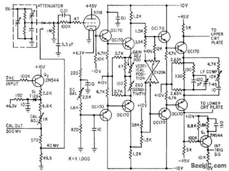
Generates 40-mv square wave at 2 kc. Provides swing of 30 v at each crt deflection plate.-O. Svehaug and J. R. Kobbe, Battery-Operated Transistor Oscilloscope,Electronics, 33:12, p 80-83. (View)
View full Circuit Diagram | Comments | Reading(1237)
GaAsFET_BIAS_SUPPLY_1
Published:2009/7/16 21:14:00 Author:Jessie
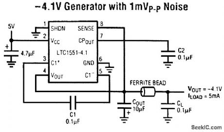
The LTC1550 and LTC1551CS8-4.1 are switched-capacitor voltage inverters that generate a regulated -4.1-V output at up to 20-mA load current. An internal linear postregulator reduces the out-put-voltage ripple to less than 1 mV, making the LTC1550 and LTC1551CS8-4.1 excellent for use as bias-voltage generators for transmitter GaAsFETs in portable RE and cellular telephone applications. The single supply voltage can range from 4.5 to 6.5 V (7 V absolute maximum). The charge pump uses four small external capacitors and operates at 900 kHz, eliminating interference with the 400-to 600-kHz IF signals commonly used in RF systems. (View)
View full Circuit Diagram | Comments | Reading(769)
| Pages:81/291 At 2081828384858687888990919293949596979899100Under 20 |
Circuit Categories
power supply circuit
Amplifier Circuit
Basic Circuit
LED and Light Circuit
Sensor Circuit
Signal Processing
Electrical Equipment Circuit
Control Circuit
Remote Control Circuit
A/D-D/A Converter Circuit
Audio Circuit
Measuring and Test Circuit
Communication Circuit
Computer-Related Circuit
555 Circuit
Automotive Circuit
Repairing Circuit