
power supply circuit
Index 89
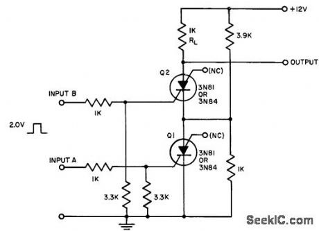
INEXPENSIVE_TWO_TRANSISTOR_XOR_GATE
Published:2009/7/16 22:28:00 Author:Jessie
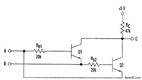
For some applications, the cost or size of XOR-gate chips can be prohibitive. One alternative is the two-transistor combination shown, which forms an inverting X0R gate for just pennies. If both inputs A and B are low, both Q1 and Q2 are off, and the output at C is high. Likewise, if both inputs are high, both transistors are turned off, and again the output at C is high. When A is high and B is low, Q1's base-emitter junction is forward-biased, while Q2's base-emitter junction is reverse-biased.This turns on Q1, pulling the output low. The last condition is B high and A low. In this state, Q1's base-emitter junction is reverse-biased, but Q2 is forward-biased. This turns on Q2 and pulls the out-put low. The sink and source currents driving the two-transistor gate are very low when the values shown are used. Even though the signals are driving the emitters of transistors, when the base and emitter are at the same potential (A and B are both high or both low), no current flows. When one of the transistors is turfted on, the emitter drive must be able to sink only the base plus collector cur-rents. This current will be approximately IE=IB+IC, where: IB≈(VH-VBE)/RB and IC≈(VCC-Vsat)/RC.From this VH+TTL high output level=3V; VBE=forward-biased base-emitter voltage ≈0.7 V;VCC=5V typical; and Vsat=0.2 V typical. Also, for this example,Rb=20 kΩ and RC=47 kΩ.Thus,IC≈215μA. (View)
View full Circuit Diagram | Comments | Reading(5582)
COINCIDENCE_DETECTOR
Published:2009/7/16 23:24:00 Author:Jessie
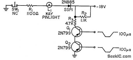
Tums on lamp to indicate coincidence of any two input pulses that are 100 microamp in amplitude and coincide for at least 1 microsec.-J. Crawling, Pulse Coincidence Defector, EEE, 11:7, p 27. (View)
View full Circuit Diagram | Comments | Reading(1547)
5_AND_33_V_SUPPLY
Published:2009/7/16 23:20:00 Author:Jessie


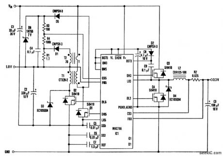
The IC shown is popular for generating 5 and 3.3 V because it includes two controllers that are highly efficient (typically >90 percent). However, the IC has a step-down (buck) topology that usually can't generate voltages equal to or higher than Vin. A four-cell NiCd or NiMH battery, for example, presents a problem because its terminal voltage can be above or below 5 V, depending on the state of its charge. This problem can be solved by designing in a flyback transformer, which allows Vin to range from 4 to 7 V. To ensure a proper gate drive to the external switching MOSFET (Q1), LX5 should be connected to ground and BST5 to the internal 5-V supply (VL) as shown. When Q1 turns on, the T1 primary current increases and stores energy in the T1 core. When Q1 turns off, the synchronous-rectifier MOSFET Q2 turns on and enables current flow to the 5-V output. For flyback circuits, Iout flows only when the rectifier conducts. Yet, IC1 is a current-mode buck regulator for which Iout must be sensed while Q1 is on. The current-sense transformer (T2), therefore, measures the T1 primary current when Q1 is on, steps down the result with a 70:1 turns ratio, and develops a voltage across resistor R1. To ensure that synchronous rectifier Q2 remains on while Q1 is off, a simple charge pump (C4 and D5) and voltage divider (R3 and R4) provide a slight offset to the current-sense signal. Thus, Q2 remains on because the IC does not detect zero output current. Vout, is regulated to 5 V,±5 percent, and the maximum Iout is 1 A over the entire Vin range. (View)
View full Circuit Diagram | Comments | Reading(902)
LCD_CONTRAST_SUPPLY
Published:2009/7/16 23:06:00 Author:Jessie
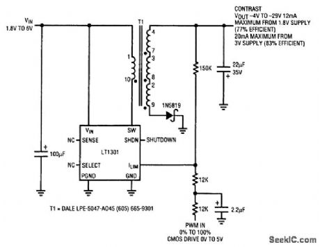
The LT1301 circuit shown generates a negative contrast voltage that may be varied from -4 to -29 V based on a PWM control signal generated by the system microprocessor. The LT1301 is a micropower switching regulator that needs only 120μA quiescent current and can be shut down to draw just 10 μA. The input supply can range from 1.8 to 6 V, making it ideal for operation from a portable battery supply. Transformer T1 is a standard four-winding transformer with independent terminal connections for each winding. Three windings are connected in series to create a 1:3 turns ratio flyback transformer. Voltage feedback is applied to the current limit input ILIM to control operation of the oscillator. A logic-level input, such as PWM generated at a microprocessor output pin or PWM circuit, sets the output voltage. As indicated, the efficiency is very good, even at low input voltages. (View)
View full Circuit Diagram | Comments | Reading(765)
PHOTOVOLTAIC_ISOLATOR_WITH_FAST_RESET
Published:2009/7/16 23:05:00 Author:Jessie
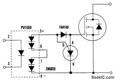
Photovoltaic isolators (PVIs) provide an isolated gate drive for MOSFETs and IGBTs. At turn-off, however, they don't pull the gate down to drain the gate charge. Using a programmable junction transistor (PUT) provides a very fast gate pull-down, pulling as much as 5 A to discharge the gate in less than 0.2 s. The PUT is a four-layer structure, much like a silicon-controlled rectifier, but with a much more sensitive anode gate. In this application, the PUT gate is driven by the PVI to a voltage equal to or greater than that of the anode that holds the PUT in the blocking state so that no current flows through the anode-cathode channel. When the PVI is turned off , the PUT gate voltage drops below the anode voltage, triggering the PUT and causing the anode-cathode channel to conduct. Conduction continues until the MOSFET gate voltage drops to about 0.5 V, at which time the PUT stops con-ducting and recovers for another cycle. (View)
View full Circuit Diagram | Comments | Reading(1980)
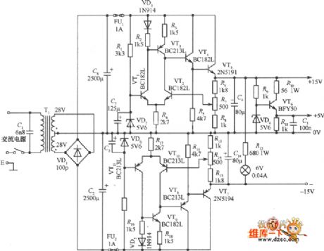
The common ±15V, 5V three kinds of output regulated power supply circuit schematic diagram
Published:2011/7/20 5:04:00 Author:nelly | Keyword: regulated power supply, output
View full Circuit Diagram | Comments | Reading(1740)
VARIABLE_VOLTAGE_SOURCE
Published:2009/7/16 23:37:00 Author:Jessie
This variable-voltage source can provide between 0.6 and 20 V, depending on the setting of R1. (View)
View full Circuit Diagram | Comments | Reading(808)
PULSE_SORTER
Published:2009/7/16 23:36:00 Author:Jessie
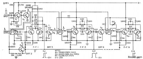
Receives train of varying width pulses and presents each pulse at output terminal corresponding lo position of pulse in train, without changing pulse widths. Three transistors and one ferrite core are used for each sorted pulse. Can handle over 1,000 pps.-J. H. Porter, Pulse Sorting with Transistors and Ferrites, Electronics, 32:20, p 64-65. (View)
View full Circuit Diagram | Comments | Reading(819)
SNUBBER_NETWORK_ENERGY_SAVER
Published:2009/7/16 23:36:00 Author:Jessie
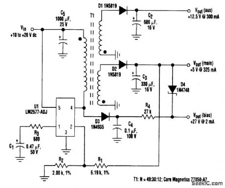
A flyback regulator offers the advantage of providing multiple output voltages with a single magnetic structure. Therefore, it is very compact and cost-effective. This particular circuit has a main +5-V output and a +12.5-V auxiliary output. The device being driven also requited a bias voltage of +27V with a few milliamperes of current. The heart of the regulator is a National Semiconductor LM2577-ADJ simple switcher controller IC, with resistors R1 and R2 providing the feedback for the rnain +5-V output. The auxiliary + 12.5-V output is regulated by the intrinsic tight coupling of a discontinuous-mode flyback topology. R3 and C1 are compensation devices. Although another winding could have been used in the transformer to provide the +27-V bias output, a free output can be realized from the transfer of the voltage spikes in the primary winding to the reservoir capacitor (C4) via diode D3. The charge in the capacitor is drawn by the current of both the bias load and the shunt zener regulator (D4). Enough charge is depleted from the capacitor to allow the next voltage spike to almost fully dump its energy in the next cycle. In a sense, this is a modified snubber network in which the energy is being put to good use, instead of being wasted as heat on a resistor. (View)
View full Circuit Diagram | Comments | Reading(2886)
RESTRICTED_RANGE_POTENTIOMETER
Published:2009/7/16 23:35:00 Author:Jessie
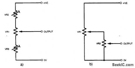
The figure shows two methods for restricting the output voltage range from a potentiometer. (View)
View full Circuit Diagram | Comments | Reading(753)
BASIC_FLYBACK_CONVERTER_CIRCUIT
Published:2009/7/16 23:35:00 Author:Jessie
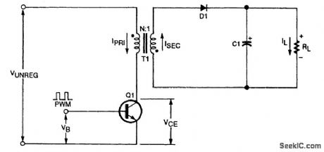
The figure shows a flyback converter, a variation on the boost regulator with a single switching transistor Q1 that eliminates the input inductor L1. This kind of off-line flyback switcher typically includes a bridge rectifier that converts the 120-Vac line voltage to 150 Vdc for the switching section. Current increases at a linear rate through the primary winding of transformer T1, which behaves like an inductor by storing energy in its core. As soon as Q1 cuts off, the magnetic field begins to collapse, and the winding polarities reverse. During the second half (flyback period), when Q1 is off, the energy is transferred to the secondary of transformer T1, charging capacitor C1 and feeding the output load. A PWM loop controls Q1's conduction by comparing output voltage to a set reference. If the load demands more current, the ON time is increased; if it demands less current, the ON time is decreased. (View)
View full Circuit Diagram | Comments | Reading(2754)
POSITION_SENSOR_POTENTIOMETER
Published:2009/7/16 23:34:00 Author:Jessie

A potentiometer can be used for position-to-voltage sensing. This figure shows the use of a po-tentiometer to sense water-level changes. (View)
View full Circuit Diagram | Comments | Reading(719)
SWITCHING_REGULATOR_WITH_TRANSFORMER_ISOLATED_FEEDBACK
Published:2009/7/16 23:34:00 Author:Jessie
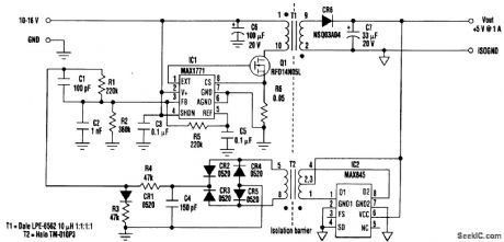
The zero (nonexistent) line regulation of a push-pull, surface-mount transformer and driver (T2 and IC2) produces an isolated feedback signal (to pin 3 of IC1) proportional to the regulator's nominal 5-V output. What results is a fully isolated dc-to-dc converter without the bandwidth constraints and aging characteristics associated with an optoisolator. By alternately grounding each end of T2's center-tapped primary, the transformer driver (IC2) generates an ac signal proportional to the desired 5-V feed-back voltage. A diode bridge (CR2 to CR5) and a capacitor (C4) convert this transformer's output to dc, and a diode-resistor network (CR1, R3, and R4) compensates for the temperature coefficient of the diode bridge. The result is a zero-TC voltage slightly less than 1/2Vout In response to a 5.00-V output, the feedback network produces an isolated 2.404 V (at IC1, pin 3) and introduces about 250 ns of delay at 100 kHz-the equivalent of 9° of phase shift. This bandwidth is sufficient for the control loop in most switching converters. Supply current for IC2 and the temperature compensation network together is about 6 mA. Starting with a 5-V, nonisolated, transformer flyback converter in which Vout connects directly to the top of C1 and R1, you can insert the isolated-feedback circuit (bottom of the figure) between Vout and C1/R1. The only modification needed to accommodate this extra isolated-feedback circuit is to reduce the value of R1, which ensures that the R1/R2 divider voltage is comparable to IC1's internal feedback reference (1.5 V). Performance of the isolated converter is virtually identical to that of the nonisolated converter, except for the power consumed by the isolated-feedback circuit.T2 provides an isolation of 500 V rms (transformers with 1500 V rms also can be obtained). (View)
View full Circuit Diagram | Comments | Reading(3079)
MISSING_PULSE_DETECTOR
Published:2009/7/16 23:34:00 Author:Jessie
Detects presence or absence of pulse train and indicates whether level remains positive or negative after pulsing stops.-R. W. Allington, Pulse Absence Detector, FEE, 11:5, p 90-91. (View)
View full Circuit Diagram | Comments | Reading(0)
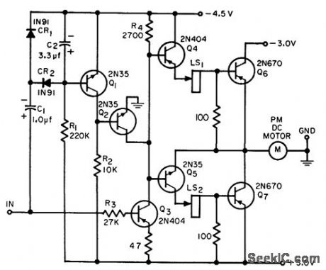
PULSE_SEQUENCE_DETECTOR
Published:2009/7/16 23:32:00 Author:Jessie
Resistor divider between Q1 and Q2 supplies current to silicon controlled switch Q1 after it is trig-gored by pulse at input A. Divider also pre vents input B from triggering Q2 until after Q1 conducts.- Transistor Manual, Seventh Edition, General Electric Co., 1964, p 428. (View)
View full Circuit Diagram | Comments | Reading(1551)
ANTICOINCIDENCE_DETECTOR
Published:2009/7/16 23:31:00 Author:Jessie
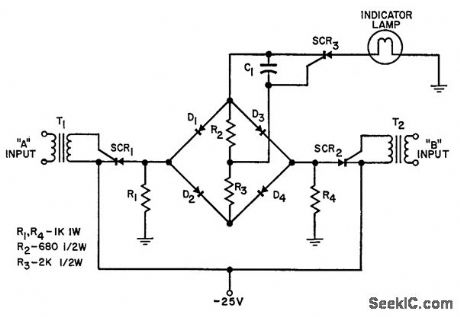
Gives indication whenever two input pulses are not coincident. Limit on smallest degree of anticoincidence that is detectable is determined by turn-on time of SCR’s, and is about 0.3 microsec for 2N1595 scr used, when C1 is omitted. Upper limit is set by C1, and can be several tenths of a second when C1 is 200 mfd. Circuit is reset by interrupting supply. Diodes are 1N691, and lamp is 1819.-J. T. Gatshal, Anti-Coincidence Detector, EEE, 10:9, p 28-29. (View)
View full Circuit Diagram | Comments | Reading(835)
_5_7AND__10V
Published:2009/7/16 23:30:00 Author:Jessie

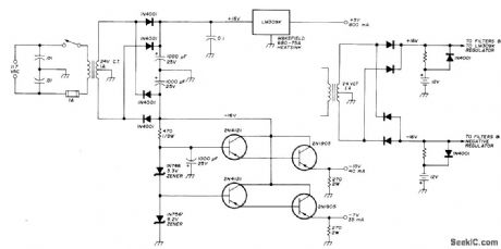
Developed to meet power requirements of RTTY message generator having ITL and Numitrons requiring +5 V and MOS RAM requiring negative voltages. Diagram shows how to add 12-V storage batteries to prevent loss of programming if AC power fails momentarily.-B, Kelley, Random Access Memory RTTY Message Generator, Ham Radio, Jan.1975, p 8-15. (View)
View full Circuit Diagram | Comments | Reading(659)
±6_V_AND_±15_V
Published:2009/7/16 23:28:00 Author:Jessie
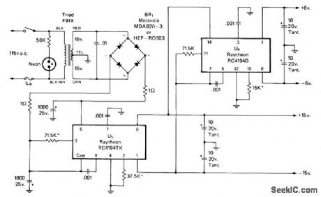
Developed for use with wide-range function generator requiring these voltages for transistors and ICs. Voltage-setting 15K and 37.5K resistors are adjusted to give de-sired output voltages.-H. Olson, The Function Generator, CQ, July 1975, p 26-28 and 71-72. (View)
View full Circuit Diagram | Comments | Reading(0)
HUMAN_BODY_MODEL
Published:2009/7/16 23:26:00 Author:Jessie

The human-body model (HBM) is approximated with a series capacitor and resistance (a); the machine model (MM) is simply a capacitor (b). The model is charged to the required test voltage (V+) and switched into the device. If the input capacitance of the device (CISS) charges to higher-than-rupture voltage, the device will be destroyed. (View)
View full Circuit Diagram | Comments | Reading(765)
PULSE_PHASE_SPLITTER_1
Published:2009/7/16 23:26:00 Author:Jessie
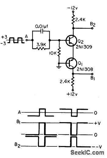
Provides bipolar pulses 180°out of phase, with perfect coincidence of negative-going trailing edges, same reference level, and drive capability for saturated inverters. Used for switching sample-hold gates requiring opposite-going pulses with trailing-edge coincidence.-G. Wolff, Simple Pulse Phase-Splitter, EEE, 14:2, p 70-72. (View)
View full Circuit Diagram | Comments | Reading(974)
| Pages:89/291 At 2081828384858687888990919293949596979899100Under 20 |
Circuit Categories
power supply circuit
Amplifier Circuit
Basic Circuit
LED and Light Circuit
Sensor Circuit
Signal Processing
Electrical Equipment Circuit
Control Circuit
Remote Control Circuit
A/D-D/A Converter Circuit
Audio Circuit
Measuring and Test Circuit
Communication Circuit
Computer-Related Circuit
555 Circuit
Automotive Circuit
Repairing Circuit