
power supply circuit
Index 92
BASIC_PUSH_PULL_CONVERTER_CIRCUIT
Published:2009/7/16 22:44:00 Author:Jessie
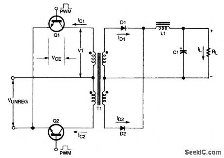
The push-pull converter consists of two forward converters working 180° out of phase. Both halves of the push-pull Converter deliver current to the load at each half cycle, and the inductor stores energy. Diodes D1 and D2 conduct simultaneously between transistor conduction, effectively short-circuiting the secondary isolation transformers. Acting as flywheel diodes, these diodes deliver useful power to the output. (View)
View full Circuit Diagram | Comments | Reading(1848)
±14_V_TRANSFORM_ERLESS
Published:2009/7/16 22:41:00 Author:Jessie
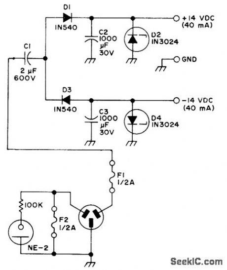
Simple low-current regulated supply requires no power transformer. Output current can be increased by using better filtering. Second ground prong is connected through fuse to grounded center conductor of AC line to guard against faulty AC wiring. If wiring is reversed, fuse will disable power supply and neon fault indicator will come on.-D. Kochen, Transformerless Power Supplies, 73 Magazine, Sept. 1971, p 14-17. (View)
View full Circuit Diagram | Comments | Reading(687)
SIMPLE_INTERCOM
Published:2009/7/16 22:41:00 Author:Jessie
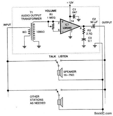
This intercom uses an LM380 IC to act as an amplifier and speaker driver (View)
View full Circuit Diagram | Comments | Reading(880)
TUNNEL_DIODE_LEVEL_DISCRIMINATOR
Published:2009/7/16 22:41:00 Author:Jessie
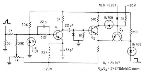
Tunnel diode at input of high-gain amplifier stage gives highly accurate trigger action even for slowly rising input pulse. Used with quinary scalers to measure time intervals accurately to within 1 nsec.-R. Englemann, Quinary Scalers: Measure Time Intervals Digitally, Electronics, 37:5, p 34-36. (View)
View full Circuit Diagram | Comments | Reading(861)
BASIC_FORWARD_CONVERTER_CIRCUIT
Published:2009/7/16 22:38:00 Author:Jessie
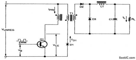
The figure is a simplified schematic for a transformer-coupled forward converter. Based on the buck converter, it is similar to the flyback converter. Inductor L1, rather than transformer T1, stores the energy. When switching transistor Q1 turns on, current builds in the primary winding of trans-former T1, storing energy. Because the secondary winding has the same polarity as the primary winding, energy is transferred forward to the output. Energy is also stored in inductor L2 through forward-biased diode D2. At this time, flywheel diode D3 is back-biased. When Q1 turns off, the transformer winding voltage reverses, back-biasing diode D2. Diode D3 becomes forward-biased, causing current to flow through RL and delivering energy to the load through inductor L1. The third winding and diode Dl return transformer T1's magnetic energy to the dc input when Q1 is off. (View)
View full Circuit Diagram | Comments | Reading(1626)
TUNNEL_DIODE_DISCRIMINATOR
Published:2009/7/16 22:38:00 Author:Jessie
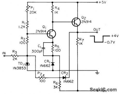
Td1, biased dose to its peak current, is connected to d-c amplifier to overcome inherent limitations of tunnel diode. When input voltage makes current through R3 exceed diode peak current, diode switches to its high-voltage state of 0.5 v. Q1 amplifies this change by factor of 10, and Q2 initiates start of square wave output. When input drops, circuit and diode revert to original state. Rise and fall times are about 10 nsec.-G. Marosi, Versatile Tunnel-Diode Discriminator, FEE, 14:5, p l20. (View)
View full Circuit Diagram | Comments | Reading(901)
125_TO_37_V_AT_15_A_
Published:2009/7/16 22:37:00 Author:Jessie
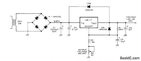
Adjustable positive voltage regulator used with simple bridge rectifier and capacitor-input filter delivers wide range of regulated voltages, all with current and thermal overload protection. Load regulation is about 0.3%.-H. Berlin, A Simple Adjustable IC Power Supply, Ham Radio, Jan. 1978, p 95. (View)
View full Circuit Diagram | Comments | Reading(1059)
FIVE_OUTPUT_CONVERTER
Published:2009/7/16 22:37:00 Author:Jessie
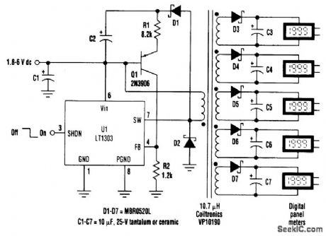
Digital panel meters (DPMs) make excellent displays for instruments and test equipment, but they suffer from one major flaw: They require a floating power supply, usually in the form of a 9-V battery. This circuit powers up to five meters from a single 1.8- to 6-V source. Each of the five outputs is fully floating, isolated, and independent in every respect. The converter is based on a flyback design, and it uses a micropower, high-efficiency regulator (LT1303) and an off-the-shelf, surface-mount inductor. The coil has six identical windings and is high-voltage-tested to 500 V rms-more than adequate isolation for the application. Operation is as follows: Feedback is extracted from the primary by Q1, which samples the flyback pedestal during the switch-off time. Typical DPMs draw approximately 1-mA supply current. The primary also is loaded with 1 mA for optimum regulation and ripple. Snubbing components, a necessity in most flyback circuits, are obviated by the action of C1 and C2. The converter also can be used with a battery. In this case, a sixth panel meter can be powered by the primary across C2. All that is required to balance the load current is to increase R1 and R2 by a factor of 10. Although this circuit is set up for 9-V output (actually 9.3 V), some DPMs need 5 or 7 V. As a result, a 4.3- or 6.2-kΩ resistor should be used in place of R1 for these voltages. The output voltage is set by R1 = (Vout-0.7)/1 mA. If any outputs aren't needed, omit the associated components and parallel the unused winding with the primary, observing the phasing. With each output loaded at 1 mA, the input current is 16.5 mA on a 5-V supply. This figure rises to about 45 mA on a 1.8-V (two-cell) input. (View)
View full Circuit Diagram | Comments | Reading(1063)
BACKUP_SUPPLY_CAPACITOR
Published:2009/7/16 22:35:00 Author:Jessie
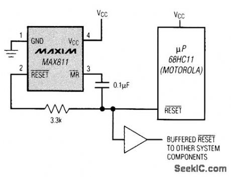
These connections allow dual control of the buffered RESET line and extend the duration of resets issued by the μP. The parts shown are CMOS RAM. (View)
View full Circuit Diagram | Comments | Reading(681)
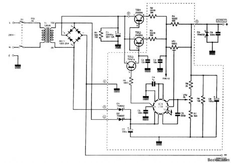
80_V_AT_15_A_FOR_COLOR_TV
Published:2009/7/17 0:13:00 Author:Jessie
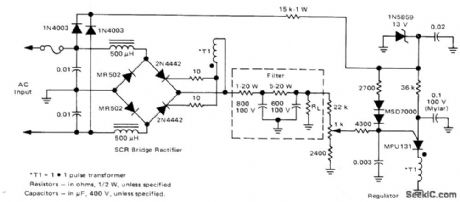
Holds output voltage across RL within 2% over line-voltage range of 105 to 140 V. Designed for use in 19-inch color TV receiver having 700-V fly back horizontal system. Bridge rectifier has two 2N4442 SCRs that control amount of output voltage by using variable duty cycle. Regulator uses MPU131 programmable UJT, which also serves for gating SCRs. 1K pot provides control of PUT gate voltage, which in turn determines output voltage across RL.-R. J. Valentine, A Low-Cost 80 V-1.5 A Color TV Power Supply, Motorola, Phoenix, AZ, 1974, AN-725, p 2. (View)
View full Circuit Diagram | Comments | Reading(819)
12_V_AT_1_A
Published:2009/7/17 1:16:00 Author:Jessie
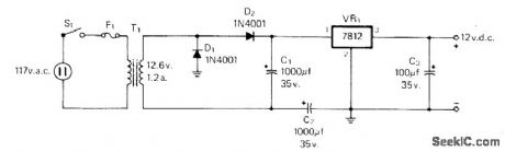
Simple supply furnishes up to 1 A with excellent regulation. Bottom of chassis can be used for heatsink. Connect additional 0.1-μF capacitor between pin 1 of VR1 and ground. T1 is Radio Shack 273-1505 with 12.6-V CT 1.2-A secondary, and F1 is 0.5-A fuse.-A. Pike, Radio Shack Power Supply, CQ, Sept.1977, p 66. (View)
View full Circuit Diagram | Comments | Reading(1151)
±0_TO_15V_AT_200mA_AND_38_TO_5V_AT_2A
Published:2009/7/17 0:11:00 Author:Jessie
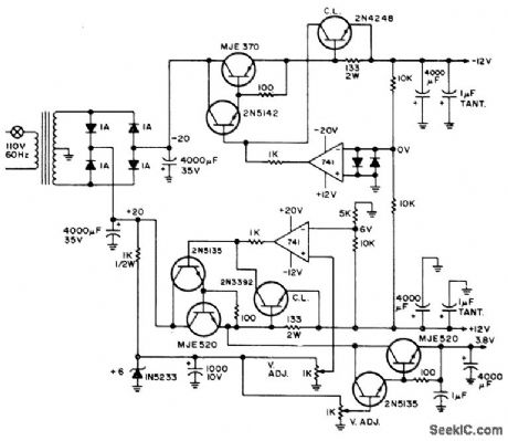
Developed for use with slow-scan television. Design provides equal positive and negative voltages that track each other with one manual control, adjustable from 0 to 15 V for opamps. Current limiting is provided for both positive and negative outputs. Low digital voltage can be adjusted to 3.8 V for RTL or 5 V for TTL, without current limiting. Use transformer having 35-V secondary, center-tapped, rated at 3 A.-D. Miller and R. Taggart, Popular SSTV Circuits, 73 Magazine, March 1973, p 55-60, 62, and 64-67. (View)
View full Circuit Diagram | Comments | Reading(1001)
±115_V
Published:2009/7/17 0:09:00 Author:Jessie

Developed for experimentation with IC audio amplifiers, delivering up to 5 W, where good regulation is required to prevent oscillation caused by feedback through power supply to input stage. Q1 and Q2 are inexpensive silicon transistors, serving also as low-cost fuse because they burn out first when power supply is overloaded. Use heatsinks with silicone grease for output transistors.-D. J. Kenney, Integrated Circuit Audio Amplifiers, 73 Magazine, Feb. 1974, p 25-30. (View)
View full Circuit Diagram | Comments | Reading(872)
ACTIVE_HIGH_Z_PROBE
Published:2009/7/16 23:52:00 Author:Jessie

This probe has a 100 mΩ input impedance and uses a T1 TLC2254 quad op amp operating from a 12 V battery.It can be used with a DVM or an analog multimeter for measurments in the high-impedance circuits. BP1 is a Tellon standoff to ensure low leakage t the terminal. (View)
View full Circuit Diagram | Comments | Reading(2877)
75_A_12_TO_16_VDC_REGULATED_POWER_SUPPLY
Published:2009/7/16 23:46:00 Author:Jessie
This supply uses an L123 regulator IC and a pair of 2N3055 power transistors as series-pass regulators VR1 is the current limit, and VR2 is the voltage control, The 2N3055 transistors and theTIP41A should be heatsinked because up to 50 W of dissipation can Occur. (View)
View full Circuit Diagram | Comments | Reading(2550)
±5_±15_AND__30_V_
Published:2009/7/16 23:45:00 Author:Jessie
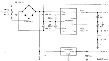
Provides all voltages needed for digitally controlled power supply that has voltage range from 0 to 25.5 V in 0.1-V increments. Highest positive voltage of +30 V is well above maximum output voltage that can be programmed.-D. Aldridge and N. Wellenstein, Designing Digitally-Controlled Power Supplies, Motorola, Phoenix, AZ, 1975, AN-703, p 4. (View)
View full Circuit Diagram | Comments | Reading(712)
SIMPLE_ADJUSTABLE_DC_SUPPLY
Published:2009/7/16 23:42:00 Author:Jessie
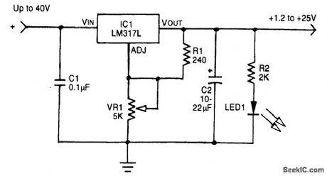
Using an LM317L IC, this regulator will find broad application where a simple adjustable supply is needed. The IC is a surface-mount type, but a different package style can be used. (View)
View full Circuit Diagram | Comments | Reading(1577)
DC_POWER_SUPPLY
Published:2009/7/16 23:42:00 Author:Jessie
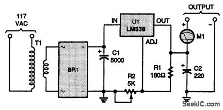
Here's the schematic for The Crusher dc power supply. The outputs are front-panel-mounted banana jacks. T1 is a 24- to 26-V transformer with 1- to 5-A capacity. C1 should be a minimum of 1000 μF per ampere of dc. C2 should be at least 100 μF (or larger). C2 helps maintain good transient response for transients that are too fast for the regulator, and 220 to 470 μF is recommended. BR1 is a 50-V bridge rectifier. U1 must be heatsinked. M1 is an ammeter of 0-5 A or 0-10 A full scale. The output voltage can be adjusted from about 1.2 to 30V via R2. Vout 1.26 (R2 /R1 + 1) volts. (View)
View full Circuit Diagram | Comments | Reading(2091)
5_AND_14_V_AT_1_A
Published:2009/7/16 23:42:00 Author:Jessie
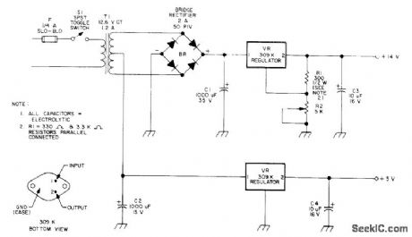
Regulated dual-voltage power supply serves for experimenting with TTL, CMOS, and linear IC projects. Higher-voltage regulator must be insulated from heat-sink.-A. Lorona, Dual Voltage Power Supply. 73 Magazine, Holiday issue 1976, p 146-147. (View)
View full Circuit Diagram | Comments | Reading(1491)
12_V_AT_5_A
Published:2009/7/16 23:40:00 Author:Jessie
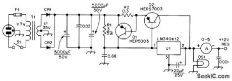
Uses National LM340K-12 mounted on external heatsink, with series-pass transistor Q2 boosting current rating to 5 A. Provides complete protection from load shorts; output drops suddenly to nearly zero when current exceeds 5 A. R2 is several feet of No, 22 enamel wound on phenolic form to make 0.3-ohm 60-W resistor. CR1 and CR2 are HEP R0103 or equivalent. Transformer is rated 18 V at 8 A.-C. R. Watts, A Crowbar-Proof 12-V Power Supply, QST, Aug. 1977, p 36-37. (View)
View full Circuit Diagram | Comments | Reading(904)
| Pages:92/291 At 2081828384858687888990919293949596979899100Under 20 |
Circuit Categories
power supply circuit
Amplifier Circuit
Basic Circuit
LED and Light Circuit
Sensor Circuit
Signal Processing
Electrical Equipment Circuit
Control Circuit
Remote Control Circuit
A/D-D/A Converter Circuit
Audio Circuit
Measuring and Test Circuit
Communication Circuit
Computer-Related Circuit
555 Circuit
Automotive Circuit
Repairing Circuit