
power supply circuit
Index 95
SIMPLE_CIRCUIT_TO_DISCONNECT_LOAD_FROM_BATTERY
Published:2009/7/17 2:31:00 Author:Jessie

To prevent battery damage, the circuit disconnects the load at a predetermined level of load voltage. This level (Vtrip, closely proportional to the battery voltage) is determined by R1 and R2 so that the voltage at pin 3 of IC1 equals 1.15 V: Vtrip = 1.15 V(R1 + R2) /R1 The allowed range for Vtrip is 2 V to 16.5 V. The load-battery connection remains open until the system receives a manual reset command. Pressing Reset (or pulling pin 3 above 1.15 V with a transistor) reconnects the load after the battery is recharged or replaced. Battery drain with the load disconnected is only 5 μA, so the circuit can remain in that state for an extended period without causing a deep discharge of the battery. Choose Q1 for a minimal voltage drop (source to drain) at the required load current. (View)
View full Circuit Diagram | Comments | Reading(1824)
OLD_TIME_RADIO
Published:2009/7/17 2:30:00 Author:Jessie
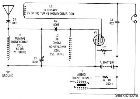
This circuit was used in the early days of radio to receive signals. Almost any battery-operated triode, such as a type 30, can be used. A battery is 3 V, R2 is a 100-Ω rheostat. Coils are typically 2 to 3 diameter honeycomb wound. (View)
View full Circuit Diagram | Comments | Reading(873)
REVERSED_POWER_SUPPLY_PROTECTOR_CIRCUIT
Published:2009/7/17 2:29:00 Author:Jessie
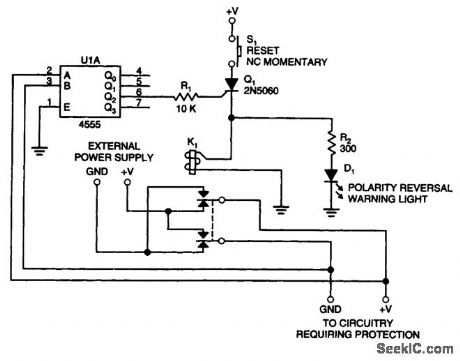
This circuit is designed to sense a power-supply output (to other circuitry) and detect a reversed-polarity condition. The circuit consists of a complementary metal-oxide semiconductor (CMOS) decoder (CD4555B), which monitors the output of an external power supply for proper polarity. If the power-supply polarity is incorrect, the CD4555B detects that condition and triggers a 2N5060 SCR (Q1). After triggering, the SCR supplies current to a relay (K1), which, upon activation, changes the external power-supply connections (to the external circuitry) to the correct polarity and illuminates a light-emitting diode (LED) to provide a visual warning of the polarity-reversal condition. After the reversed-polarity condition is remedied, pressing the contact switch (S1) momentarily will reset the circuit to its original state. In its present configuration, the circuit can accommodate standard positive power supplies with dc voltages of +5, +10, + 12, and + 15 V. The decoder was designed to operate at these different voltages. With some modifications, the circuit can monitor and correct anomalous power-supply outputs from +3 V, +28 V, or negative-polarity power supplies, or voltages that are either too high or too low. (View)
View full Circuit Diagram | Comments | Reading(859)
LONGWAVE_TRF_TUNER
Published:2009/7/17 2:29:00 Author:Jessie
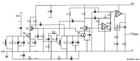
This TRF tuner was intended for reception of Radio 4 AM broadcast signals in the United Kingdom on 198 kHz, with the best possible audio fidelity. It can be used as an IF amplifier or for reception of LW or MW AM broadcasts in other areas. The aerial wire is directly connected, via SK1, to the input tuned circuit (coil L1 and capacitors VC1 and C3) via a small-value capacitor C1. The second tuned circuit (L2, VC2, and C8) is similarly connected to the output from transistor TR2. The output from transistor TR3 is taken to the op-amp demodulator (IC1a) and also, via capacitor C9, to the diode-pump circuit D1/D2. The pump is used to generate a small negative AGC. For AM detection, if a diode is used as the rectifier, the tuner will not work very well on input volt-ages less than 0.5V peak. However, if a pair of diodes are hooked around an op amp, IC1a, as shown in the figure, the rectification threshold is reduced to a few millivolts, which increases the demodulator sensitivity by a few hundred times. The other half of the dual op amp, IC1b, is a straight AP amplifying stage, whose gain is adjustable by potentiometer VR1. Resistor R13 and capacitor C10, on its noninverting input (pin 5), act as a simple RE filter to remove any residual 198-kHz signal voltage from the audio output.
(View)
View full Circuit Diagram | Comments | Reading(1572)
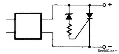
SIMPLE_REVERSE_POLARITY_PROTECTION_CIRCUITS
Published:2009/7/17 2:29:00 Author:Jessie
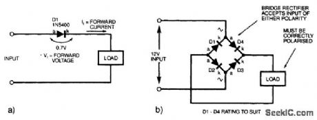
Two methods to avoid damage to circuitry from reverse voltages using diodes are shown. (View)
View full Circuit Diagram | Comments | Reading(956)
MOV_SURGE_PROTECTION_CIRCUIT
Published:2009/7/17 2:28:00 Author:Jessie
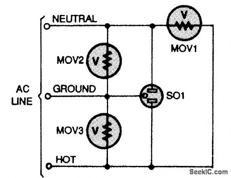
Three MOV devices (connected as shown) provide superior protection against line surges because all three legs are protected against excessive potential differences. (View)
View full Circuit Diagram | Comments | Reading(3147)
SHORT_CIRCUIT_SHUTDOWN_CIRCUIT
Published:2009/7/17 2:27:00 Author:Jessie

When a short or severe undervoltage develops, Q1 is cut off, deenergizing Q1, and disconnecting the load from the power supply. (View)
View full Circuit Diagram | Comments | Reading(867)
SIMPLE_CROWBAR_CIRCUIT
Published:2009/7/17 2:27:00 Author:Jessie
This circuit uses a zener diode and an SCR. When the supply voltage exceeds the zener break-down voltage plus the gate turn-on voltage of the SCR, current flows in the gate circuit, turning on the SCR and effectively shorting the supply. A fuse is generally placed in the supply line; it is designed to blow when the SCR fires, protecting and shutting down the supply. (View)
View full Circuit Diagram | Comments | Reading(1318)
ELECTROSTATIC_PROTECTOR
Published:2009/7/17 2:27:00 Author:Jessie

A simple way to protect the gate of a power MOS device is to place back-to-back zener diodes between the device's gate and source (a). The breakdown voltage of the zeners is chosen to be less than the oxide-rupture voltage so that the ESD transient cannot harm the gate. The resistance of the clamp diodes must be kept to a minimum because ESD transients can have high peak currents (in amps), and the voltage appearing at the gate will be the sum of the zener breakdown voltage and the IR voltage drop across the diode resistance. The machine model (MM) is particularly stressful because there is no resistance to limit the current. Along with the diodes, the resistor (RG) is added to improve MM performance. RG prevents the gate of the MOSFET from charging to a dangerous voltage level during the time the ESD transient is dissipated by the diodes. A machine model here is defined as a 200-pF capacitor with no series resistance. (View)
View full Circuit Diagram | Comments | Reading(1066)
OVER_UNDERVOLTAGE_PROTECTOR
Published:2009/7/17 2:26:00 Author:Jessie

The ICL7665 over/undervoltage detector manufactured by Maxim (IC1) monitors the line voltage and disconnects the load if the input voltage goes below 95 V or above 130 V. The over/under-voltage detector (IC1) monitors the filtered, unregulated dc voltage developed across C5, which changes with the input line voltage. The input voltage levels to IC1 are set by resistors R2 through R8. As long as the voltage at pin 3 is above 1.3 V and the voltage at pin 6 is lower than 1.3 V, both outputs (pins 1 and 7) are low and RY1 is turned on and its contacts are closed. The average line voltage varies at different locations. Trimmer potentiometer R4 provides a small adjustment range so that you can set the window's center for your particular line voltage. When IC1 detects an overvoltage at pin 3, it immediately opens the relay by sending a high output to pin 2 of NOR gate IC3-a, which, in turn, turns off Q1. When IC1 detects an overvoltage at pin 6, the output at pin 7 goes high. Monostable multivibrator IC2 provides a 1/2-s delay to keep RY1 turned off long enough for the voltage across C5 to return to normal. When pin 7 of IC1 goes high, it triggers IC2, and the high output at pin 6 of IC2 causes the output of NOR gate IC3-a to go low, which turns Q1 off and deenergizes RY1. Switch S2 lets you quickly check the circuit's operation at any time. Pushing S2 raises the voltage at the junction of R2 and R5 and turns RY1 off. RESET switch S1 restores normal operation. Switch S1 turns the circuit on initially. An LM7805 voltage regulator (IC4) provides a constant 5-V supply for the integrated circuits and the relay control current. (View)
View full Circuit Diagram | Comments | Reading(1309)
TUNABLE_PHASE_SHIFT_NETWORK
Published:2009/7/17 2:25:00 Author:Jessie
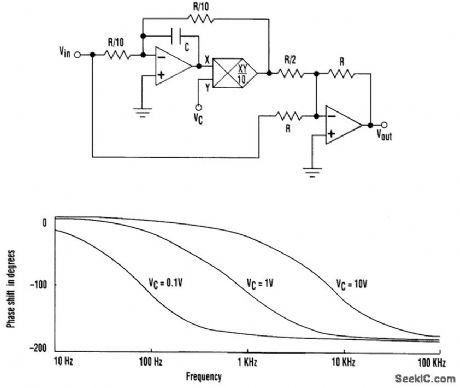
Frequently, the need arises to control the phase shift or delay of an audio signal. The all-pass active filter shown performs this function. The transfer function has the form
T(S)=Vout (S)/Vin(S)=1-sRC/Vc/(1+sRC/Vc)
where Vc is the control voltage and Vc > 0. As a result, this filter has unity voltage gain for all frequencies. Vc can be used to vary the phase over the theoretical range from -180°≤φ≤0. In the circuit, the left op amp and analog multiplied combination produce an inverting, first-order, low-pass filter whose pole frequency is set by the control voltage, according to ωp=VC/RC. An MC1495 analog multiplier has an adjustable scale factor, which, in this case, is set to 0.1 for convenience. Choosing a center frequency of fo at the geometric mean of the audio range, or fo= √20×20KΩ=633 Hz, centers the phase shift at -90°. For VC=1Vdc, using the relationship fo-VCωo/2π=VC/2πRC sets the RC time constant to 252μs. Selecting R 10 kΩ makes C 25 nF. (View)
View full Circuit Diagram | Comments | Reading(982)
DELAYED_ACTION_MOBILE_RADIO_PROTECTION_CIRCUIT
Published:2009/7/17 2:23:00 Author:Jessie
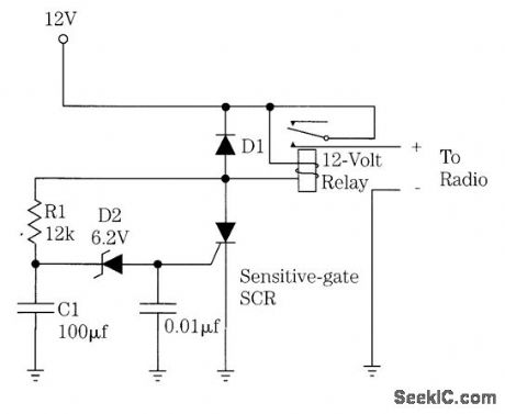
This circuit uses an SCR and an RC circuit to delay application of power to a mobile radio or other equipment. This is to provide protection from starting motor- and alternator-induced transients. (View)
View full Circuit Diagram | Comments | Reading(693)
1_TRANSISTOR_REGENERATIVE_RECEIVER
Published:2009/7/17 2:22:00 Author:Jessie
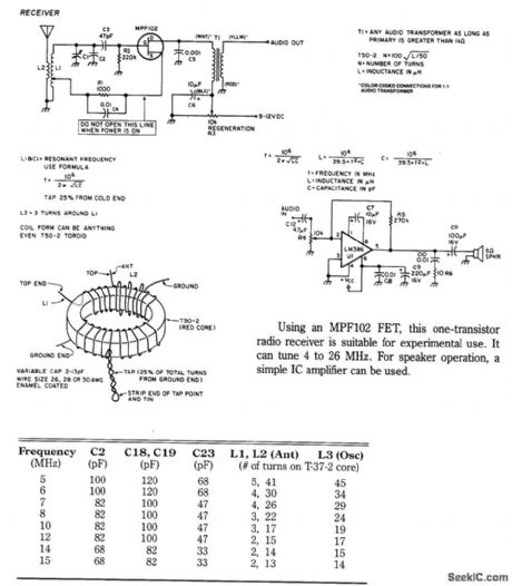
Using an MPF102 FET, this one-transistor radio receiver is suitable for experimental use. It can tune 4 to 26 MHz. For speaker operation, a simple IC amplifier can be used. (View)
View full Circuit Diagram | Comments | Reading(4450)
12_V_AT_150_mA
Published:2009/7/17 2:21:00 Author:Jessie
Designed for use with audio preamρs, FM tuners, and stereo decoders for which minimum ripple, minimum noise, good regulation, and good temperature stability are important. Uses 5.6-V reference zener that is fed from output but is inside feedback loop. Un-regulated input can be up to 36 V.-M. L. Old-field, Regulated Power Supplies, Wireless World, Nov. 1972, p 520-521. (View)
View full Circuit Diagram | Comments | Reading(755)
126_V_AT_3_A_1
Published:2009/7/17 2:20:00 Author:Jessie
Will handle typical 15-W 2-m transceiver Short-circuit protection is provided by 82-ohm resistor Adjust value of resistor marked 2.4K to give desired output voltage Transformer secondary is nominally 35 V center-tapρed at 1.5 A Output capacitor can be tantalum-slug electrolytic with any value above 10 μF.-H. H. Cross, The Chintzy 12, 73 Magazine, Feb. 1977, p 40-41. (View)
View full Circuit Diagram | Comments | Reading(740)
DIODE_RELAY_DRIVER_PROTECTION
Published:2009/7/17 2:19:00 Author:Jessie
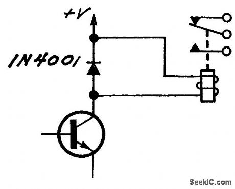
The diode protects the switching transistor from the voltage spike caused by the relay coil. (View)
View full Circuit Diagram | Comments | Reading(885)
MEASURING_TRANSISTOR_SHORT_CIRCUIT_INPUT_RESISTANCE
Published:2009/7/17 2:16:00 Author:Jessie
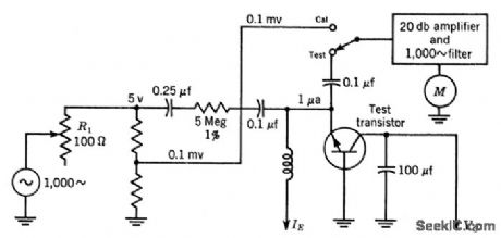
Output meter gives direct reading of h-ib when input current is held at 1 microamp.-Texas Instruments Inc., Transistor Circuit Design, McGraw-Hill, N.Y., 1963, p 70. (View)
View full Circuit Diagram | Comments | Reading(737)
MEASURING_TRANSISTOR_TRANSFER_RATIO
Published:2009/7/17 2:15:00 Author:Jessie
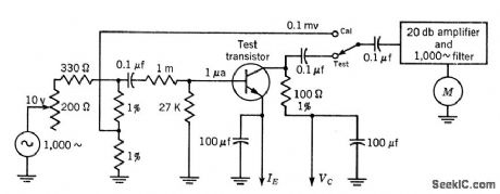
Basic test circuit shown measures small-signal short-circuit forward current transfer ratio of transistors. Gives direct reading of h-fe when base current is held at fixed value of 1 microamp.-Texas Instruments Inc., Transistor Circuit Design, McGraw-Hill, N.Y., 1963, p 70. (View)
View full Circuit Diagram | Comments | Reading(930)
THERMAL_CONSTANTS_OF_TRANSISTORS
Published:2009/7/17 2:14:00 Author:Jessie
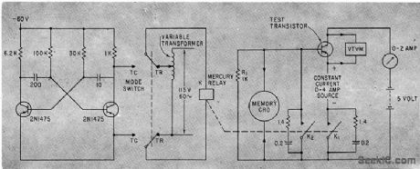
Astable mvbr generates 0.3-sec pulse every 3 sec to drive mercury relay when mode switch is on IC contacts for measuring thermal lime constant of transistor under test. Constant power is applied between pulses, using cro as guide for keeping power level near normal steady-state value of transistor. Thermal resistance data is obtained with mode switch on contact TR, where 60-cps supply drives relay.-H. Bauman, Practical Way to Measure Transistor Thermal Resistance, Electronics, 36:7, p 66-67. (View)
View full Circuit Diagram | Comments | Reading(783)
MOISTURE_METER
Published:2009/7/17 2:13:00 Author:Jessie
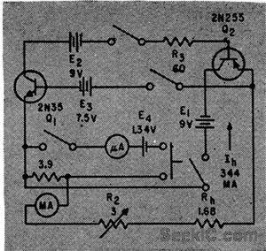
Maintains constant current for 20 minutes of heavy loading of conventional zinc-carbon dry cells when measuring moisture in pulverized coal or other powders, through use of inverse voltage feedback in two-stage direct-coupled amplifier.-G. E. Fasching, Inverse Feedback Stabilizes Dry Cell Current Sources, Electronics, 32:41, p 78. (View)
View full Circuit Diagram | Comments | Reading(867)
| Pages:95/291 At 2081828384858687888990919293949596979899100Under 20 |
Circuit Categories
power supply circuit
Amplifier Circuit
Basic Circuit
LED and Light Circuit
Sensor Circuit
Signal Processing
Electrical Equipment Circuit
Control Circuit
Remote Control Circuit
A/D-D/A Converter Circuit
Audio Circuit
Measuring and Test Circuit
Communication Circuit
Computer-Related Circuit
555 Circuit
Automotive Circuit
Repairing Circuit