
power supply circuit
Index 93
1_MILLISEC_TO_30_HOURS
Published:2009/7/17 1:38:00 Author:Jessie
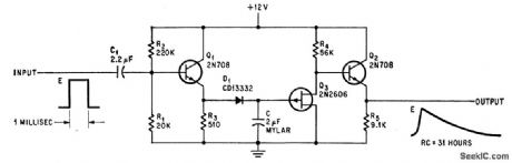
Input and out-put emitter-followers isolate fat, Extremely low lockage current through D1 and fet Q3 give circuit 30-hour time constant.-M. E. McGee, FET Circuit Stretches 1-MSEC Pulse to 30 Hours, Electronics, 38:7, p 87-88. (View)
View full Circuit Diagram | Comments | Reading(693)
LOGIC_PROBE_CIRCUIT
Published:2009/7/17 1:35:00 Author:Jessie
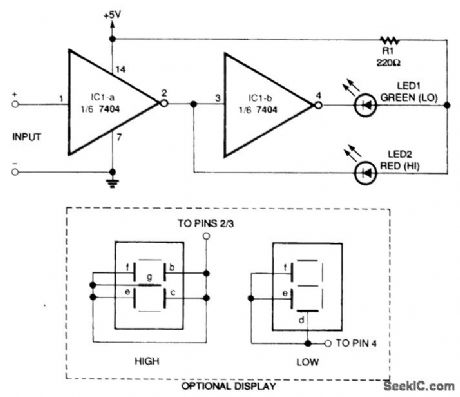
In this logic probe circuit, the red LED indicates logic high and the green indicates logic low, The optional use of an LED seven-segment readout is also shown. (View)
View full Circuit Diagram | Comments | Reading(1953)
CONVEYOR_BELT_OVERLOAD_PROTECTION
Published:2009/7/17 1:29:00 Author:Jessie
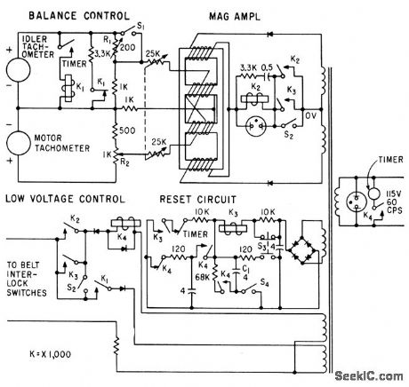
Tachometers monitor belt slip and feed four-leg magnetic amplifier which controls conveyor drive relay K2. If tachometer outputs do not match because of belt slip or belt failure, bridge becomes unbalanced, magamp output decreases, and K2 drops out.-F. R. Hulscher, Fail-Safe Circuits for Conveyor Sys tems, Electronics, 32:28, p 60. (View)
View full Circuit Diagram | Comments | Reading(1398)
INFRARED_LOGIC_PROBE
Published:2009/7/17 1:29:00 Author:Jessie
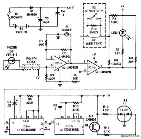
Infrared light detected by photodiode D2 is amplified by IC1-a. The value of R2 can be changed to decrease the sensitivity of the circuit, if your application demands it. Connector J1 provides an output to an oscilloscope for the display of the amplified photodiode signal. This is handy when checking the pulsed emitters in most remote controls. Voltage comparator IC1-b squares up signals from IC1-a to digital logic levels for IC2-a. LED1 and current-limiting resistor R7 indicate the presence of steady-state infrared and also function with pulsed emitters if the duty cycle is appropriate Monostable multivibrator IC2 conditions pulse trains with any period shorter than the time constant of R9 and C1 into a low-frequency waveform with a very high duty cycle. This provides pulses for LED2 that are constant in frequency and duty cycle, regardless of the high input frequency to IC2-a.Any frequency input to IC2-a with a period longer than the time constant of R9 and C1 creates IC2-b output pulses with the same width as before at the input frequency. Tricolor LED2 (a dual red/green device) functions as a pilot lamp and indicator for pulsed infrared sources. LED2 will always glow red and pulse amber (red + green) when infrared pulses are detected. The power source for the circuit is a 9-V battery. Alkaline batteries will provide many hours of operation because the circuit has low-power integrated circuits in place of S2 for most emitters. For certain devices, such as slotted optical switches, CD laser diodes, and reflective sensors, more sensitivity might be desirable. If you plan to use the probe for LEDs that operate below 0.5 mW, install S2 and R13-if not, you can in-stall a wire jumper on the board instead of the switch. (View)
View full Circuit Diagram | Comments | Reading(1015)
CMOS_INTERFACE
Published:2009/7/17 1:27:00 Author:Jessie

This CMOS interface makes it possible for a simple or complex analog circuit to input data into a digital system. (View)
View full Circuit Diagram | Comments | Reading(793)
75_W_INSTANT_START_BALLAST_
Published:2009/7/12 22:10:00 Author:May

DC voltage for 20-kHz two-transistor oscillatoris obtained from AC line, Secondaryis added to centertapρed tank coil of T1Bto provide 1 kV P starting voltage required by 96-inch instantstart lamps.Artide gives transformer and choke winding data along with circuit details and performance data. Lamps operate independently, so one stays on when other is removed.-R. J. Haver, The Verdict Is In: Solid-State Fluorescent Ballasts Are Here, EDN Magazine, Nov. 5, 1976, p 65-69. (View)
View full Circuit Diagram | Comments | Reading(911)
G_M_DRIVE_FOR_SCALE_OF_64_COUNTER
Published:2009/7/17 1:37:00 Author:Jessie

Shapes pulses from Geiger-Muller tube and uses one-shot mvbr to drive first scaling stage.-F. E. Armstrong, Battery Powered Portable Staler, Electronics, 33:19, p 74-75. (View)
View full Circuit Diagram | Comments | Reading(646)
MINI_HIGH_VOLTAGE_PROBE
Published:2009/7/17 1:37:00 Author:Jessie
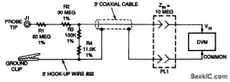
The schematic diagram of the probe reveals its simple circuit. It is a standard voltage divider made up of resistors with a 1-percent tolerance. Resistors R1 and R2 are the key elements here. They are rated at 15,000 V and 10,000 V, respectively. The 7500-Vdc peak specification for the assembled probe must not be exceeded under any circumstances! The values for series resistors R3 and R4 are in parallel with the 10-MΩ resistance of the DVM, thus providing a 1000-to-1 voltage divider. Voltage measurements made by the probe should be multiplied by a factor of 1000. If your DVM uses an input impedance different from the standard 10 MΩ, you can adjust the R3/R4 series combination, as needed. (View)
View full Circuit Diagram | Comments | Reading(1118)
±12_V
Published:2009/7/17 1:36:00 Author:Jessie

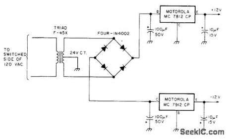
Simple circuit provides power required for two 741 opamps used in CRT tuning indicator circuit for RTTY receiver.-R. R. Parry, RTTY CRT Tuning Indicator, 73 Magazine, Sept. 1977, p 118-120. (View)
View full Circuit Diagram | Comments | Reading(1240)
PREFERRED_PULSE_SHAPER
Published:2009/7/17 1:36:00 Author:Jessie

Generally used with monostable mvbr to form 1-microsec pulse at end of delay period. Also used to reshape pulse that has suffered deterioration by passage through long chain of gates, or to produce 1.microsec pulse whose leading edge coincides with trailing edge of a positive pulse, for delaying output by width of input pulse.-NBS, Handbook Preferred Circuits Navy Aeronautical Electronic Equipment, Vol. 11, Semiconductor Device Circuits, PSC 11 (originally PC 214), p 11-2. (View)
View full Circuit Diagram | Comments | Reading(815)
LOGIC_PROBE_
Published:2009/7/17 1:34:00 Author:Jessie

The figure shows the schematic for a versatile logic probe. The zener diode clamps the input signal just above the TTL inverter's 2.2-V trigger voltage. Zener diode D1 can be left out if the probe is going to be used only on TTL circuits. The logic probe is based mainly on inverters IC1-a and IC1-b, which are sections of a 7404 integrated circuit. Depending on whether the input is high or low, the inverters enable AND gate IC2-a or IC2-b, each of which is a section of a 4081. Each AND gate is connected to an oscillator, one low-frequency, the other high. When an AND gate is made high, it passes the frequency of its oscillator to the piezo buzzer (BZ1). Whenever a high is at the input, the buzzer will produce the high tone; whenever a low is at the input, the buzzer will sound the low tone. With switch S2 in the PULSE position, if pulses are present at the input, a yellow LED will light and the buzzer will sound at the frequency of the pulses. The CMOS/TTL switch selects the voltage from the circuit under test or the voltage from the 78L05 regulator. Note that when this switch is in the TTL position, it can work only with 5-Vdc, but when the switch is in the CMOS position, it can work with from 7.5 to 35 Vdc. (View)
View full Circuit Diagram | Comments | Reading(4477)
_13_V_AT_1_A
Published:2009/7/17 1:31:00 Author:Jessie
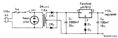
Regulated output voltage can be varied upward about 0.6 V per diode by placing silicon diodes between pin 3 and ground. Two diodes boost output of regulator from 11.9 V to about 13 V. Insulate regulator from heatsink with mica washers. CR1 and CR2 are 50-PIV 3-A diodes. Motorola equivalent of regulator is MC7812.-A. M. Clarke, Simple, Super regulated, 12 Volt Supply, CQ, April 1974, p 61-62. (View)
View full Circuit Diagram | Comments | Reading(891)
SEVEN_SEGMENT_LOGIC_PROBE
Published:2009/7/17 1:29:00 Author:Jessie
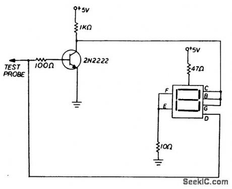
This circuit is capable of indicating the HI or LO status of a digital circuit. The circuit in the figure will display the letter H for HI or +5 V and L for LO or 0 V. The 2N2222 NPN transistor serves as a driver for turning on the appropriate segments of the display, thereby producing the letter H. This condition will occur with a + 5-V signal applied to the base of the transistor. If a 0-V signal is detected at the base of the transistor, the letter L will be displayed, indicating that the transistor driver is turned off. (View)
View full Circuit Diagram | Comments | Reading(1025)
SCOPE_PROBE_CIRCUITS
Published:2009/7/17 1:40:00 Author:Jessie
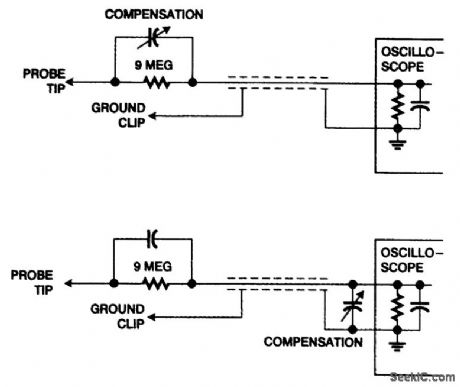
Assuming a 1-MΩ Scope input impedance and input capacitance Cin, Ccompensation=(Rprobe/1 MΩ) Cprobe or Cprobe /Cinput = Rinput/Rprobe. (View)
View full Circuit Diagram | Comments | Reading(803)
NONDIFFERENTIAL_MAGNETIC_INVERTER
Published:2009/7/17 1:45:00 Author:Jessie
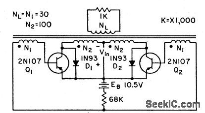
Is analogous to free-running capacitor-coupled mvbr. Frequency and output amplitude are both directly proportional to input voltage. Chief drawback is need to increase input voltage to get higher frequency, which in turn increases all winding voltages.-J. Markus, Handbook of Electronic Control Circuits, McGraw-Hill, N.Y., 1959, p 102. (View)
View full Circuit Diagram | Comments | Reading(774)
PULSE_FORMER_AND_SHAPER
Published:2009/7/17 1:44:00 Author:Jessie
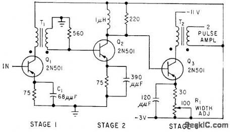
Converts sine-wave input to 40 millimicrosec output. Used in versatile pulse generator for testing high-speed computer circuits. Input frequency range is 3 to 20 Mg.-L. Numann Transistorized Generator for Pulse Circuit Design, Electronics, 32:14, p 47-49. (View)
View full Circuit Diagram | Comments | Reading(695)
FET_CONVERTS_TRIANGULAR_TO_SINE
Published:2009/7/17 1:43:00 Author:Jessie
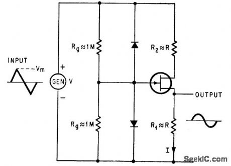
Eliminates need for signal rectification by using symmetrical properties of Fairchild FSB40 fet with respect to source and drain. For p-channel units, reverse the diodes.-R. D. Middlebrook and 1. Richer, Nonreactive Filter Converts Triangular Waves to Sines Electronits, 38:5, p 96-101. (View)
View full Circuit Diagram | Comments | Reading(907)
_5_V_AT_425_mA_
Published:2009/7/17 1:42:00 Author:Jessie
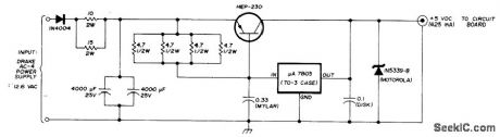
Developed for syllabic VOX system used with Drake T-4XB and R-4B transmitter and receiver. Input is taken from 12.6-VAC transformer winding of power supply for Drake, so equipment power switch also turns off 5-V supply. - R.W. Hitchcock, Syllabic VOX System for Drake Equipment, Ham Radio, Aug. 1976, p 24-29. (View)
View full Circuit Diagram | Comments | Reading(758)
DOUBLE_BRIDGE_OPEN_FUSE_DETECTOR
Published:2009/7/17 1:42:00 Author:Jessie
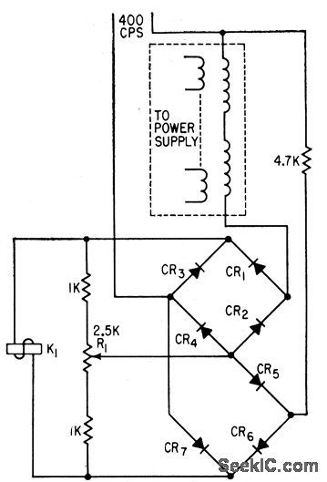
Used with magnetic amplifier to disconnect d-c voltage from section protected by fuse that opens. Output of lower bridge is balanced against output of upper bridge by adjusting R1. Gives greatly increased sensitivity.-J. Maroz, Magnetic Amplifier Detects Open Fuses, Electronics, 31:29, p 86-92. (View)
View full Circuit Diagram | Comments | Reading(728)
BATTERY_SWlTCH_OFF
Published:2009/7/12 21:39:00 Author:May
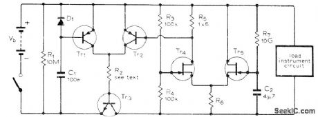
Can be added to any battery-operated device to eliminate unnecessary running down of costly batteries when someone forgets to tum switch off manually. Circuit shown gives operating time of about 10 hours ,permitting use of equipment for full working day without interruption. Normal operation can be restored after shut-off byturning manual switch off and then on again. When circuit has switched off, only battery drain is current through 10-megohm resistor R1 and leakage through transistors. Time of switch-off can be changed by altering C2 or R7. Tr1 and Tr2 are 2N4061, BC478, or similar PNP silicon; Tr3 is 2N3053, BC142, or similar medium-power NPN silicon; Tr4 and Tr5 are 2N3819; D1 is any small silicon diode; R6 is 4.7K for 9-V or 12-V battery, and 10K for 15-V to 27-V battery. R2 is chosen to suit working current and battery voltage; suitable value is 15Vb/Iout.-D, T. Smith, Automatic Battery Switch-Off Circuit, Wireless World, April 1976, p 76.
(View)
View full Circuit Diagram | Comments | Reading(1258)
| Pages:93/291 At 2081828384858687888990919293949596979899100Under 20 |
Circuit Categories
power supply circuit
Amplifier Circuit
Basic Circuit
LED and Light Circuit
Sensor Circuit
Signal Processing
Electrical Equipment Circuit
Control Circuit
Remote Control Circuit
A/D-D/A Converter Circuit
Audio Circuit
Measuring and Test Circuit
Communication Circuit
Computer-Related Circuit
555 Circuit
Automotive Circuit
Repairing Circuit