
power supply circuit
Index 83
REPEATER_EMERGENCT_POWER_SUPPLY
Published:2009/7/12 23:06:00 Author:May
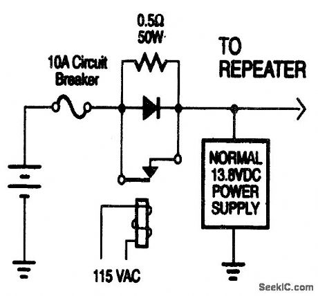
If your repeater needs emergency power, this circuit might do. Connect a 12-V storage battery, a relay, and a 0.5-Ω 50-W resistor as shown. Normally, the battery charges at a low rate (less than 1 A) through the 0.5-Ω resistor. When power fails, current can flow from the battery through the diode for a few milliseconds, until the relay drops out and closes the contacts, completely eliminating any voltage drop. If your repeater doesn't use a 13.8-V power supply, you could purchase a 2-A battery charger and connect a 0.5- to l-Ω resistor (50 W) in series with the battery. This will charge at approximately 1/2 A and maintain the battery. (View)
View full Circuit Diagram | Comments | Reading(903)
2_m_HT_BASE_STATION_ADAPTER
Published:2009/7/12 23:02:00 Author:May
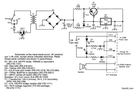
This device mates with a small handie-talkie (HT) and provides power and speaker interface as well as charging capability. It was designed for an Icom 02-AT, but can be adapted for other HTs as well.
(View)
View full Circuit Diagram | Comments | Reading(1212)
VOLTAGE_CONTROLLED_PRR
Published:2009/7/16 21:05:00 Author:Jessie
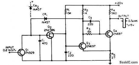
Input change of only 0.5 v will change pulse repetition rate of generator by factor of more than 1 to 10,000,000. Output pulse is about 0.3 microsec wide, with rise and fall limes of 20 nsec. Addition of back-biased diode CR2 extends low-frequency limit below 0.05 pps.-G. Richwell, Wide-Range Voltage-Controlled Pulse Generator, EEE, 13:10, p 72-77.
(View)
View full Circuit Diagram | Comments | Reading(825)
ADJUSTABLE_SWITCHED_REGIJLATOR
Published:2009/7/16 21:04:00 Author:Jessie
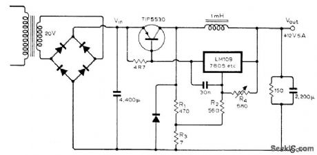
Circuit shows method of using LM109, 7805, or other IC voltage regulator to provide output voltage that is higher than rated output of IC. Voltage pedestal is developed across R2 and R3 for adding to normal regulated output of IC. R4 adjusts amount of added voltage. Divider R1-R2 provides positive feedback into pedestal circuit of regulator, to allow switching of IC and transistor.-V. R. Krause, Adjustable Voltage-Switching Regulator, Wireless World, May 1976, p 80. (View)
View full Circuit Diagram | Comments | Reading(3414)
STROBE_POWER_SUPPLY
Published:2009/7/16 21:04:00 Author:Jessie
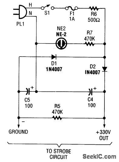
This 330-V power supply is a simple voltage doubler which provides 330 Vdc for a strobe circuit. This supply is not isolated from the power lines and extreme caution is advised. (View)
View full Circuit Diagram | Comments | Reading(859)
ALIGNMENT_CORRECTION
Published:2009/7/16 21:04:00 Author:Jessie
Circuit developed for correcting alignment inaccuracies between electrostatic deflection plates and face of cathode-ray tube gives output varying from 0 to +3.5 V when input varies from 0 to-4 v.-F.E. Smith, Buffer Amplifier Supplies Bipolar Output,Electronics, 37:21, p 75. (View)
View full Circuit Diagram | Comments | Reading(873)
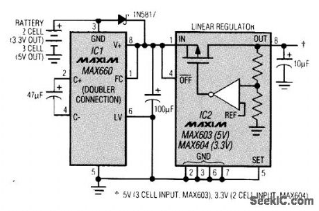
GaAsFET_BIAS_SUPPLY
Published:2009/7/16 21:03:00 Author:Jessie
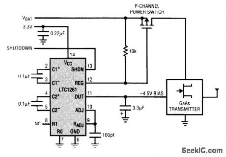
Cellular telephones and other mobile communications gear use depletion-mode GaAsFET RE output transistors, which require a negative bias voltage for proper operation. This LTC1261 circuit generates a regulated negative voltage using no inductors, and will give plenty of drive for GaAsFET bias circuits. The LTC1261CS8 inverts the supply voltage (5 V to -4.5 V), whereas the LTC1261CS can invert or double the supply voltage (3 V to -4 or -5 V). Both parts regulate the generated output voltage. The quiescent current is just 600 μA, and the shutdown current is only 5 μA. The combination of high oscillator frequency, which reduces the switched capacitor size, and the variety of fixed-output regulated negative voltages allows for a minimum-space power supply. The LTC1261 comparator output controls a P-channel MOSFET to ensure that the drain current for the GaAsFET is switched off until the regulated negative output voltage is valid. This ensures that the gate voltage is sufficient to keep the GaAsFET off during power-up, preventing unsaturated operation and excessive operation. (View)
View full Circuit Diagram | Comments | Reading(1005)
HIGH_VOLTAGE_GENERATOR
Published:2009/7/16 21:03:00 Author:Jessie
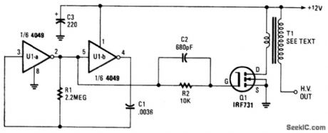
A 4049 Hex inverter drives an IRF731 hex FET. The 4049 is configured as an oscillator. Q1 should be heatsinked. T1 is an auto ignition coil. (View)
View full Circuit Diagram | Comments | Reading(3523)
CHARGE_PUMP_BOOST_CONVERTER
Published:2009/7/16 21:03:00 Author:Jessie
The circuit overcomes the charge pump's lack of regulation by adding a regulator externally. Another option-if load currents are modest-is to add regulation on the chip. Regulation in a monolithic chip is generally accomplished either as linear regulation or as charge-pump modulation. Linear regulation offers lower output noise; therefore, provides better performance in (for example) a GaAsFET-bias circuit for RF amplifiers. Charge-pump modulation (which controls the switch resistance) offers more output current for a given die size (or cost) because the IC need not include a series pass transistor. (View)
View full Circuit Diagram | Comments | Reading(975)
12_16_V_FROM_63_VAC
Published:2009/7/16 21:02:00 Author:Jessie
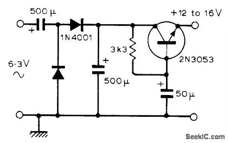
Designed for use with transistor or IC amplifier being fed by tube-type preamp having 6.3-V power transformer winding for filament supply. - K. D. James; Balanced Output Amplifier, Wireless World, Dec.1975, p 576. (View)
View full Circuit Diagram | Comments | Reading(809)
BASIC_STEP_UP_OUTPUT_STAGE_OF_A_DC_TO_DC_CONVERTER
Published:2009/7/16 21:02:00 Author:Jessie
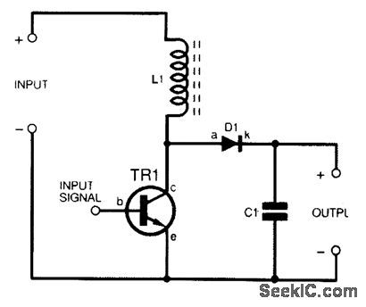
This figure shows the basic circuit configuration for a step-up output stage. (View)
View full Circuit Diagram | Comments | Reading(759)
HIGH_VOLTAGE_PULSE_SUPPLY
Published:2009/7/16 21:02:00 Author:Jessie
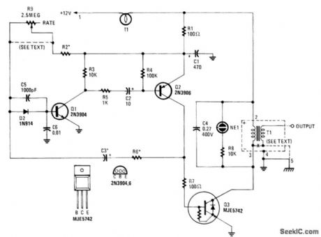
This high-voltage pulse supply will generate pulses up to 30 kV. Q1 and Q2 form a multivibrator in conjunction with peripheral components R1 through R6 and C1, C2, C3, C5, C6, and D2. R9 adjusts the pulse repetition rate. R2 should be selected to limit the maximum repetition rate to 20 Hz. I1 is a type 1156 lamp used as a current limiter. R9 can be left out and R2 selected to produce a fixed rate, if desired.Try about 1 MΩ as a start.Q3 serves as a power amplifier and switch to drive T1 (an automotive ignition coil). NE1 is used as a pulse indicator and indicates circuit operation. Because this circuit can develop up to 30 kV, suitable construction techniques and safety precautions should be observed. (View)
View full Circuit Diagram | Comments | Reading(1086)
STROBE_PULSE_GENERATOR
Published:2009/7/16 21:02:00 Author:Jessie
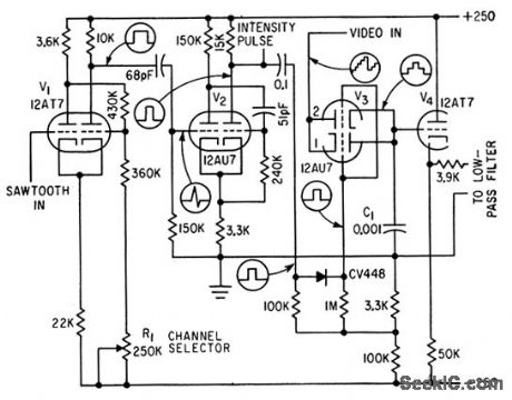
Constant-amplitude sawtooth from timebase of display unit is fed to one control grid of Schmitt trigger V1, whose output triggers one-shot mvbr to produce gating pulse 0.1 millisec wide that also identifies strobed channel on crt by brightening trace c-d that point.-A. Potton, Telemetry System for Testing Automobiles,Electronics, 33:43, p 57-59. (View)
View full Circuit Diagram | Comments | Reading(823)
±9_V
Published:2009/7/16 21:01:00 Author:Jessie
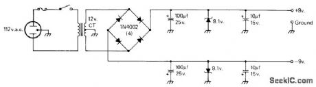
Developed for use with demodulator of teleprinter. Regulation is provided by zeners. -I. Schwartz, An RTTY Primer,CQ, Feb.1978, p 31-36. (View)
View full Circuit Diagram | Comments | Reading(921)
10000_V_STANDARD
Published:2009/7/16 21:01:00 Author:Jessie
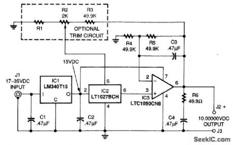
The heart of the voltage standard is the LT1027BCH voltage reference IC, IC2, manufactured by Linear Technology Corp. It sports a temperature coefficient of two parts per million per degree Celsius (2 PPM/℃), and it comes pretrimmed within ±0.05 percent. Provision for optional trim circuitry is included on the board; however, it requires an additional resistor-selection step. To eliminate sensitivity to input-voltage variations, the incoming supply is regulated at 15 Vdc. This is accomplished with a conventional LM340T15 voltage regulator, which powers both the reference IC and the output amplifier. The LT1050 amplifier doubles the 5-V output of the LT1027 to the desired 10 Vdc. It is chopper-stabilized, providing far lower drift than a conventional op amp. Noise filtering is provided by the 0.47-μF capacitor across the feedback resistor. Note that the LT1050 does not have the out-put drive of a bipolar device-thus, the slightly higher than normal feedback resistors. You should not try to use the voltage standard with loads below 10 kΩ. The 0.47-μF/49.9-Ω output network improves stability when cables and capacitive loads are driven. (View)
View full Circuit Diagram | Comments | Reading(1176)
AMPLIFIER_FOR_MARKER_GENERATOR
Published:2009/7/16 21:00:00 Author:Jessie
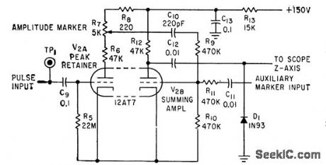
Triode V2A amplifies brightening pulse generated by marker circuit, and feeds amplified pulse to V2B for mixing with fixed or variable external marker pulse so both are applied to Z-axis of scope.-D. J. Odorizzi, Z-Axis Marker Generator for Bandpass Circuit Alignment, Electronics, 33:26, p 108-110. (View)
View full Circuit Diagram | Comments | Reading(896)
COLD_CATHODE_FLUORESCENT_LAMP_SUPPLY
Published:2009/7/16 21:00:00 Author:Jessie
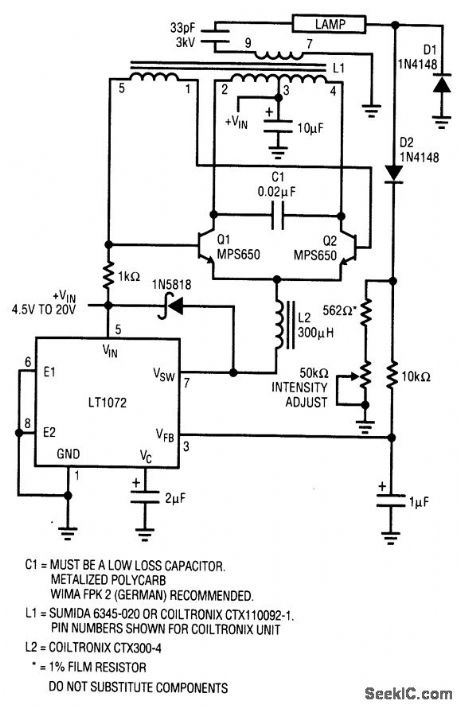
For back-lit LCD displays,this supply will drive a lamp. LT1072 drives Q1 and Q2,and a slne waveappears across C1. L1 is a transformer that steps up this voltage to about 1 400 V D1 and D2 detect lampcurrent and form a feedback loop to the LT1072 to control lamp brightness. (View)
View full Circuit Diagram | Comments | Reading(972)
40_W_120_Vac_INVERTER
Published:2009/7/16 20:59:00 Author:Jessie
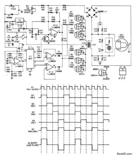
This inverter uses a 12.6-V to 120-V transformer to deliver a quasi-sine wave that has the same rms and peak voltage as a pure sine wave. Q1 to Q6 must be heatsinked. A 1.5 x4 aluminum heatsd was used on the prototype. The transformer should be a 3-A unit. The circuit uses feedback to help regulate the output voltage to 120 Vac. Notice that the output frequency is 75 Hz to avoid saturating the core of T1. (View)
View full Circuit Diagram | Comments | Reading(4898)
LOW_COST_SQUARE_WAVES
Published:2009/7/16 20:57:00 Author:Jessie

Conversion circuit coupled to sine-wave audio oscillator gives square wcnre generator at half usual cost. Will shape sine waves upto 3 Mc before trailing edges of square-wave output begin to deteriorate. Can be triggered by input signals from 0.2 to 10 v. Positive input turns on D1 and Q1, driving amplitude-limiting pair Q2-D2 into conductionto square up waveform. Lower half of circuit generates negative square pulse in negative manner.-R. S. Selleck, Converting Audio Oscillators to Square-Wave Generators, Electronics, 39:16, p 123. (View)
View full Circuit Diagram | Comments | Reading(1173)
3_A_SWITCHING_REGULATOR
Published:2009/7/16 20:57:00 Author:Jessie
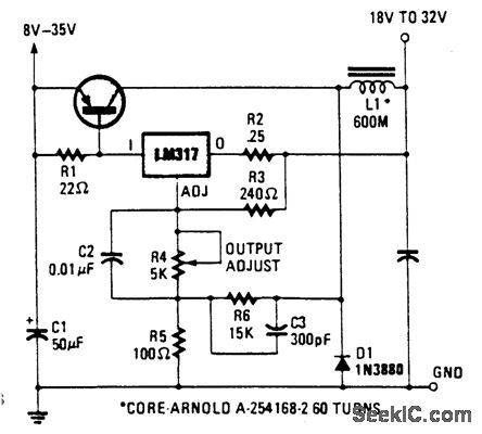
This switching regulator uses an LM317 and a pnp switching transistor of 3-to 5-A rating. L1 is wound on a commercially available core. (View)
View full Circuit Diagram | Comments | Reading(1359)
| Pages:83/291 At 2081828384858687888990919293949596979899100Under 20 |
Circuit Categories
power supply circuit
Amplifier Circuit
Basic Circuit
LED and Light Circuit
Sensor Circuit
Signal Processing
Electrical Equipment Circuit
Control Circuit
Remote Control Circuit
A/D-D/A Converter Circuit
Audio Circuit
Measuring and Test Circuit
Communication Circuit
Computer-Related Circuit
555 Circuit
Automotive Circuit
Repairing Circuit