
power supply circuit
Index 82
VOLTAGE_PROGRAMMABLE_CURRENT_SOURCE
Published:2009/7/16 21:14:00 Author:Jessie
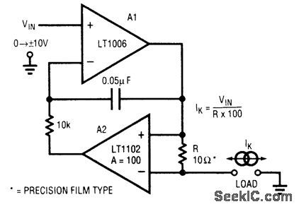
This circuit is a programmable current source in which op amp LT1102 (Linear Technology Corp.) is used in conjunction with LT1006 op amp. A1, biased by Vin, drives current through R (10Ω) and the load. A2 senses this current and controls A1. The 10-kΩ resistor and 0.05-μF capacitor sets the frequency response of the circuit.
(View)
View full Circuit Diagram | Comments | Reading(3685)
TRANSFORMERLESS_POWER_SUPPLY
Published:2009/7/16 21:13:00 Author:Jessie
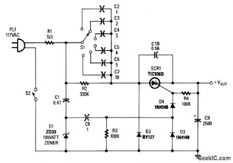
By selecting capacitors, various voltages can be obtained from this supply. Notice that C2 through C7 must be nonpolarized capacitors, such as oil-filled or foil types (Mylar) rated for at least 250 Vac.
Warning: This supply is not isolated from the ac mains and presents a serious safety hazard if body contact is made anywhere to this circuit or anything that is powered by it. Use only for applications where contact is avoided or impossible. (View)
View full Circuit Diagram | Comments | Reading(2106)
33_V_7_A_SUPPLY
Published:2009/7/16 21:12:00 Author:Jessie
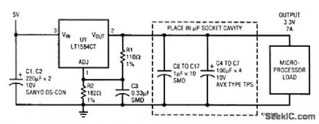
Many microprocessor systems use 3.3-V microprocessors, cache RAM, and chip sets. This system configuration increases the current requirements of the 3.3-V supply. In addition, many of these microprocessors have a stop-clock feature for power savings, which introduces a load-current step to the power supply. Adjustable regulators are recommended for microprocessors that have power-saving (stop-clock) modes. The circuit shown has good transient response to load steps for most 3.3-V microprocessors. An external capacitor at the ADJUST pin can reduce the total filter capacitance required by one half to take care of large load transients. (View)
View full Circuit Diagram | Comments | Reading(720)
SWITCH_SELECTED_FIXED_VOLTAGE_POWER_SUPPLY
Published:2009/7/16 21:12:00 Author:Jessie
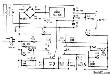
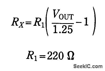
This supply can serve as a battery eliminator for various devices (such as tape recorders, small radios, clocks, etc.).
S1 selects a resistance that is predetermined to provide a preselected output voltage. In this circuit, various conunonly used supply voltages produced by batteries were chosen, but any voltages up to the rating of T1 (approximately) can be produced by choosing an appropriate resistor.
The resistor value is given by:
Remember to provide adequate heatsinking for U1. (View)
View full Circuit Diagram | Comments | Reading(966)
FLASH_MEMORY_Vpp_GENERATOR
Published:2009/7/16 21:12:00 Author:Jessie
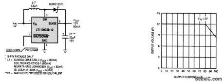
Generating 12 V for flash memory programming is a common requirement in portable systems and PCMIA cards. The LT1109-12 dc-to-dc converter simplifies this task and uses only 0.75 in2 of PC board space. The LT1109-12 is offered in an eight-lead SO package and requires only three other surface-mount components to construct a complete 12-Vpp generator. At 12 V, 60 mA of programming current is produced, enough for simultaneous programming of two flash memories. The circuit draws 320 μA (max.) of standby current while shut down and provides a clean transition from 5 to 12 V at its output with no overshoot. (View)
View full Circuit Diagram | Comments | Reading(856)
TRACE_INTENSIFIER
Published:2009/7/16 21:11:00 Author:Jessie

Designed to convert weak positive-going pulse lo negative-going pulse with 15 v minimum amplitude, as required on cathode of A-scope radar presentation on commercial oscilloscope. Minimum input amplitude is 250 mv.-L.J. Brocato, Scope-Trace Intensification Converter,EEE,13:2,p 62-63. (View)
View full Circuit Diagram | Comments | Reading(853)
SCR_VARIABLE_dc_POWER_SUPPLY
Published:2009/7/16 21:11:00 Author:Jessie
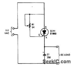
By adjusting the SCR trigger point, a form of phase control can be obtained from an SCR, which produces a dc output, depending on the conduction angle. (View)
View full Circuit Diagram | Comments | Reading(1498)
STEP_VARIABLE_dc_SUPPLY
Published:2009/7/16 21:10:00 Author:Jessie
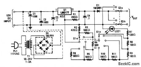
Intended as a replacement for generally poorly regulated wall-type ac/dc adapters, this circuit offers superior performance to simple, unregulated adapters. Voltages of 3, 6, 9, and 12 V are available. The DPDT switch serves as a polarity-reversal switch. R2 through R6 can be replaced with a 2.5-kΩ pot for a variable voltage of 1 to 12 V. R7 through R10 can be replaced by a fixed resistor of about 1 kΩ if the LED1 brightness variation with output voltage is not a problem. (View)
View full Circuit Diagram | Comments | Reading(860)
N85403-switching power supply thick film integrated circuit
Published:2011/7/27 10:36:00 Author:Nancy | Keyword: switching power supply, thick film
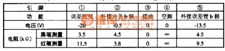
The N85403 is a switching power supply thick film integrated circuit widely used in the West Lake series (such as 54 CD8A) color TV.
1. Functions and features:The N85403 integrated circuit contains error control circuit, error sampling voltage processing circuit and some other auxiliary function circuits.
2. Pin functions and data:The N85403 integrated circuit adopts 5-pin SIP structure, the pin function and data of the integrated circuit is shown as the table.
Tips: The voltage to earth of the integrated circuit is measured by using pin 3 as the ground. (View)
View full Circuit Diagram | Comments | Reading(595)
DUAL_O_to_50_V_5_A_UNIVERSAL_POWER_SUPPLY
Published:2009/7/16 21:09:00 Author:Jessie
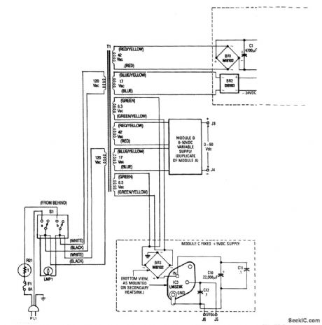
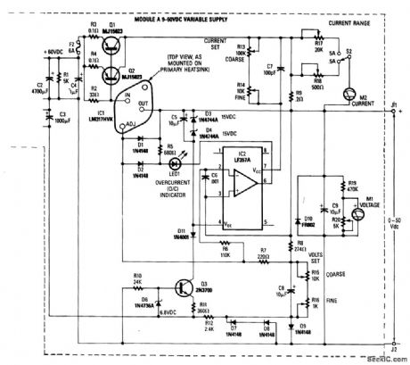
T1 has two primaries and six secondaries; the two 120-VAC primaries and 6.3-VAC secondaries are in parallel. Modules A and B are identical; hence, only Module A's parts are called out. Module C is wired point-to-point on the IC3 heatsink. (View)
View full Circuit Diagram | Comments | Reading(1370)
LM317_CIRCUIT
Published:2009/7/16 21:09:00 Author:Jessie
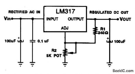
The figure shows a typical simplified wiring diagram. Note that the output voltage is determined by resistors R1 and R2 (the value of R2 is recommended to be around 240 Ω). The regulated output voltage is given by the formula Vout =1.25 (1 +R2/R1). (View)
View full Circuit Diagram | Comments | Reading(1167)
RASTER_HORIZONTAL_SWEEP_GENERATOR
Published:2009/7/16 21:09:00 Author:Jessie
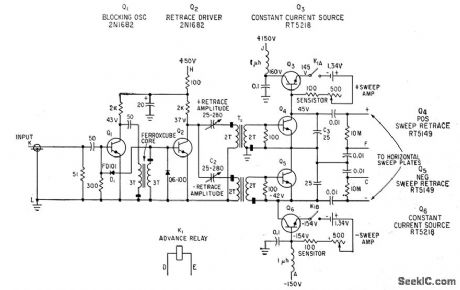
Input from 400-kc timing generator triggers Q4 through Q2 and T1,making C3 discharge to Provide sweep retrace, Negative sweep is similar except that capacitor is charged from minus 150 v.-R. P. Rufer and W.A. Karlotski, Use Raster Oscilloscopes for Faster Time Measurements,Electronics,35 52,p 38-42. (View)
View full Circuit Diagram | Comments | Reading(1105)
AMPLITUDE_DISCRIMINATOR
Published:2009/7/16 21:08:00 Author:Jessie
Used in nuclear physics to determine whether voltage or current input pulse is above or below predetermined level. Triggering threshold is set by adjusting bias of diode D1. Accuracy is within 1 microamp at 50-microamp triggering level, or within 0.4 mv at 10-my triggering level-F. S. Goulding and L. B. Robinson, Achieving Discriminator Levels with a Biased Input Diode, Electronics, 33:21, p 89-91. (View)
View full Circuit Diagram | Comments | Reading(0)
NEGATIVE_REGULATOR
Published:2009/7/16 21:07:00 Author:Jessie

Regulating negative voltages with minimal dropout is now possible with the LT1185 universal voltage regulator. It supplies up to 3 A of output current with a dropout voltage guaranteed to be less than 1.2 V. The five-lead TO-220 package includes a pin that allows accurate current-limit adjustment for lower-current applications. Although aimed primarily at negative regulation applications, the LT1185 works equally well as a floating positive regulator. Output voltage is programmable from 2.3 to 30 V. (View)
View full Circuit Diagram | Comments | Reading(1257)
14_V_AT_250mA_FOR_CASSETTE_DECK
Published:2009/7/16 21:07:00 Author:Jessie
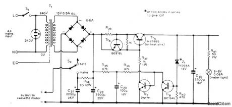
Used in high-quality stereo cassette deck operating from AC line or battery. For U.S. applications, use 120-V power transformer. Power for cassette motor is taken directly from power-supply filter capacitors through 20-ohm 10-W resistor, with negative return line connecting directly to filter capacitors instead of chassis, to eliminate noise originating from pulsating current of cassette-drive motor-control circuit. Article gives all other circuits of cassette deck and describes operation in detail.-J. L. Linsley Hood, Low-Noise, Low-cost Cassette Deck, Wireless World, Part 2 - June 1976, p 62-66 (Part1 - May 1976, p 36-40;Part 3 – Aug. 1976,p 55-56). (View)
View full Circuit Diagram | Comments | Reading(1838)
UHF_SYNCHRONIZER
Published:2009/7/16 21:06:00 Author:Jessie
Simple tunnel-diode circuit can synchronize any scope to any constant frequency up to signal-bondwidth limits of scope, even though bandwidths are greater than cro sync circuits can handle. Upper frequency limit of circuit is at least 1.2 gc. Diode oscillates at frequency controlled primarily by L1, but will lock onto uhf input signal and deliver exact subharmonic of input. Can provide countdowns at ratios exceeding 100:1.-F.M. Carlson,Tunnel- Diodo UHF Synchronizer, EEE, 12:2, p 109. (View)
View full Circuit Diagram | Comments | Reading(768)
RASTER_VERTICAL_TRIGGERING_GENERATOR
Published:2009/7/16 21:06:00 Author:Jessie
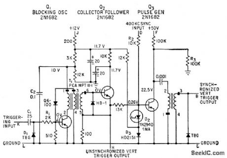
Output pulse width of blocking oscillator Q1 is over 3.5 microsec, determined by T1 and C2.Q2 couples this pulse to output H for use as unsynchronized output, while 03 with 400-kc sync input serves with D2 as coincidence gate to give output only when both sync and gate pulses are present-R. P. Ruler and W. A. Karlotski, Use Raster Oscilloscopes for Faster Time Measurements, Electronics, 35:52, p 38-42. (View)
View full Circuit Diagram | Comments | Reading(798)
25_A_125_to_25_V_REGULATED_POWER_SUPPLY
Published:2009/7/16 21:05:00 Author:Jessie
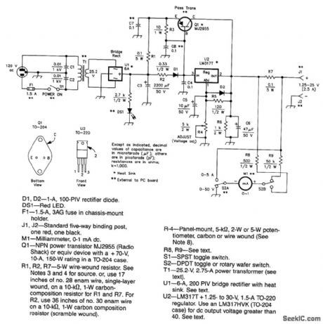
This power supply uses an LM317J adjustable regulator and an MJ2955 pass transistor, Q1 and U2 as well as U1 should be heatsinked. A suitable heatsink would typically be 4 x4 x 1 fins, extruded type, because up to 65 W dissipation can occur. R8 and R9 should be 1% types or selected from 5% film types with an accurate ohmmeter. Capacitors are disc ceramic except for those with polarity marked, which are electrolytic. (View)
View full Circuit Diagram | Comments | Reading(1836)
35_V_7_A_LINEAR_REGULATOR_SUPPLY
Published:2009/7/16 21:05:00 Author:Jessie
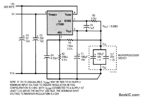
The LT1580 linear regulator circuit shown achieves ±2 percent dc output-voltage accuracy at up to 7 A load current. This circuit restricts the output-voltage transients because of 200-mA to 4-A load-current steps to 65 mV p-p. The LT1580 has a separate remote sense input that maintains the dc voltage at the load accurately, independent of the load current. Output-voltage variation over the full load-current range, known as Load regulation, with remote sense connected (R3 = 0Ω) is very close to ±0 percent. The LT1580 transient response to 3.8-A-load current steps is 88.7 mV p-p (R3 = 0Ω). Resistor R3 is added to intentionally introduce some dc load regulation. The feedback resistors are chosen to set the no-load output voltage slightly higher than 3.5 V. At 4-A load current, the output voltage is regulated slightly below 3.5 V. (View)
View full Circuit Diagram | Comments | Reading(789)
15V_AT_1_A
Published:2009/7/16 21:05:00 Author:Jessie
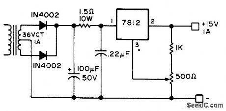
Developed for operating CRO from AC line. Can also be used for recharging batteries of portable CRO if pot is set to correct charging voltage for cells being used. Use good heat-sink with 7812 regulator.-G. E. Friton, Eyes for Your Shack, 73 Magazine, Jan.1976, p 66-69.
(View)
View full Circuit Diagram | Comments | Reading(1807)
| Pages:82/291 At 2081828384858687888990919293949596979899100Under 20 |
Circuit Categories
power supply circuit
Amplifier Circuit
Basic Circuit
LED and Light Circuit
Sensor Circuit
Signal Processing
Electrical Equipment Circuit
Control Circuit
Remote Control Circuit
A/D-D/A Converter Circuit
Audio Circuit
Measuring and Test Circuit
Communication Circuit
Computer-Related Circuit
555 Circuit
Automotive Circuit
Repairing Circuit