
power supply circuit
Index 84
GELECTRONIC_DESIGN
Published:2009/7/16 20:56:00 Author:Jessie
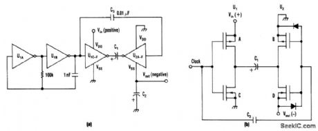

Using a charge pump and oscillator, this circuit uses a 7-kHz oscillator. When the clock is high, C and D are on, grounding the positive side of C1 and making negative voltage available at the VSS terminal of U2.With C= C1 + C2, the p-p output ripple is:
Converter output impedance is about 100Ω and maximum current is 10 mA dc. (View)
View full Circuit Diagram | Comments | Reading(753)
PPI_GROUND_PULSE_BLANKER
Published:2009/7/16 20:56:00 Author:Jessie
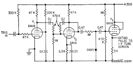
Used in backscatter receiver to produce gating pulse that can be applied to screen grid of final i-f stage to remove bright ground pulse (occurring because receiver is fed from transmitting antenna by way of transmit-receive switch)from ppi screen.-K. Perry, Reducing Interference in lonospheric Sounding, 33:22, Electronics, p 118-120. (View)
View full Circuit Diagram | Comments | Reading(680)
AUDIBLE_VOLTMETER
Published:2009/7/16 20:55:00 Author:Jessie
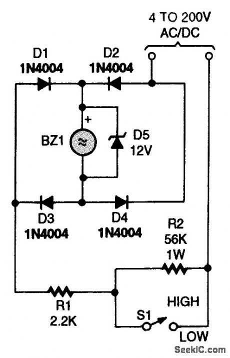
The audible voltmeter can be used to test for ac or dc voltages in a circuit. With S1 closed, the circuit can be used to test for voltages between 4 and 24 V. When S1 is open, it can be used to check for the presence of voltages of up to 200 V (View)
View full Circuit Diagram | Comments | Reading(2010)
ASTABLE_HYBRID_TD_TRANSISTOR_SQUARE_WAVE_GENERATOR
Published:2009/7/16 20:54:00 Author:Jessie
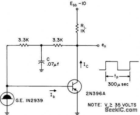
Fast switching capability of tunnel diode contributes to clean output waveform of mvbr configuration.- Trcmsistor Manual, Sevenlh Edition, General Electric Co.,1964, p 367. (View)
View full Circuit Diagram | Comments | Reading(747)
ISOLATED_15_V_TO_2_500_V_SUPPLY
Published:2009/7/16 20:54:00 Author:Jessie
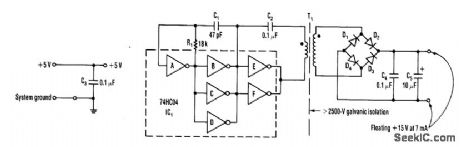
A dc-dc converter using a 74HC04 drives T1. T1 is a ferrite-core transformer using a Fair-Rite, Inc. P/N 5975000201 (μo + 5 000) and has a 7-turn primary and a 25-tum secondary. Kynar, #30 wirewrap wire is used. With T1, the circuit isolation is good to 2 500 V. (View)
View full Circuit Diagram | Comments | Reading(832)
INDUCTORLESS_BIPOLAR_SUPPLY_GENERATOR
Published:2009/7/16 20:54:00 Author:Jessie
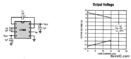
Localized generation of bipolar supply rails is useful in many op-amp, data-conversion, and interface applications. To avoid the design time and effort of putting together a switching regulator circuit, switched-capacitor conversion should be considered as a simple, effective alternative. The LT1026 is shown here in a useful application circuit that can generate rail voltages of both polarities from a 5-V logic supply. Output voltage will vary with load (as shown on the graph), from ±9 V at minimal load currents to ±6 V at a load current of 15 mA. These boosted rails can be used to extend comrnon-mode input and output ranges of circuits without doing level shifting, ac coupling, or signal clipping. Because the LT1026 is supplied in an eight-lead SO package, the entire circuit can be surface-mounted using tantalum or ceramic capacitors. (View)
View full Circuit Diagram | Comments | Reading(950)
INVERTER_OUTPUT_STAGE_OF_A_DC_TO_DC_CONVERTER
Published:2009/7/16 20:53:00 Author:Jessie
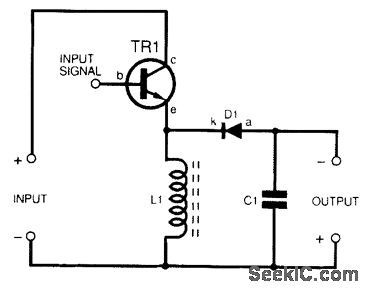
This figure shows the circuit diagram for an inverter output stage. (View)
View full Circuit Diagram | Comments | Reading(713)
20_μA_QUIESCENT_CURRENT_REGULATOR
Published:2009/7/16 20:53:00 Author:Jessie
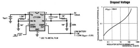
Knowing when the battery voltage is getting low allows equipment to arrange time to save valuable information. The LT1120A not only provides micropower, low-dropout regulation, but also includes a tow-battery detection comparator, all in an eight-lead DIP or SO package. The LT1120A supplies up to 125 mA at regulated voltages from 2.5 to 20 V. The low dropout voltage of 0.6 V (max.) lowers the battery input voltage requirements, and the small 40-μA (max.) quiescent current extends battery life. The LT1120A has yet more functions. The logic-compatible SHUTDOWN pin removes power to the load. The precision 2.5-V reference has the ability to both sink and source current to supply low-power backup circuits. Also, the LT1120A's design prevents excessive current draw when in dropout. (View)
View full Circuit Diagram | Comments | Reading(730)
100_W_SINE_AT_60_Hz
Published:2009/7/12 22:46:00 Author:May
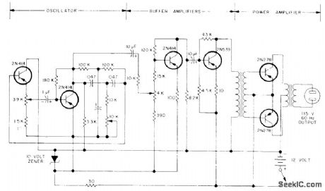
Consists essentially of 60-Hz sine-wave oscillator with 10K frequency-control pot, two buffer stages, and push-pull power amplifier. Circuit eliminates noise problems of square-wave inverters when operating 115-V radio receiver or cassette player in car.- G. C. Ford, Power Inverter with Sine Wave Output, 73 Magazine, May 1973, p 29-32. (View)
View full Circuit Diagram | Comments | Reading(3640)
2_V_REFERENCE
Published:2009/7/16 20:52:00 Author:Jessie
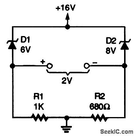
Zener diodes that operate below the 3- or 4-V level do not perform as well as higher-voltage zeners, and are not normally used for low-voltage references. The 2-V reference uses two higher-voltage zeners, D1 and D2, to obtain a stable operating reference voltage. Any possible voltage changes from temperature variations are almost completely canceled out with the two-zener circuit, making it a more accurate reference source than a circuit with a single zener. Other low-reference -voltage sources can be created by substituting different-valued zeners for D1 and D2. (View)
View full Circuit Diagram | Comments | Reading(892)
TONAL_VOLTMETER
Published:2009/7/16 20:52:00 Author:Jessie
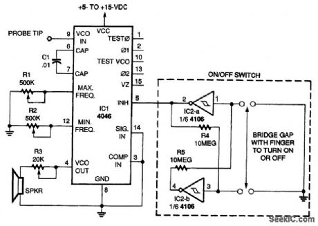
The circuit is based on a CD4046B phase-locked loop (PLL) IC with a built-in voltage-controlled oscillator (VCO). The frequency of the VCO is determined by the voltage at pin 9, capacitor C1 between pins 6 and 7, and potentiometer R2 at pin 12, which sets the tonal voltmeter's minimum frequency. The VCO output, which appears at pin 4, is normally fed back into the comparator in-put at pin 3. However, in this circuit, the VCO output drives a speaker directly. The VCO operates while the inhibit line (INH) at pin 5 is held logic low, and it turns off when INH is logic high. A touch switch consisting of two Schmitt-trigger inverters (IC2-a and IC2-b) turns the circuit on and off to conserve power when the TVM is not being used. The touch switch can be replaced with a standard SPST switch, if so desired. This is recommended if you don't have a Schmitt-trigger inverter and don't want to purchase one. The tonal voltmeter emits a low tone when reading a logic low. As the voltage input increases, the tone pitch increases until the input voltage reaches a logic high. As the voltage input decreases, the pitch decreases. (View)
View full Circuit Diagram | Comments | Reading(1735)
DIODE_CMOS_STABILIZER
Published:2009/7/16 20:52:00 Author:Jessie

The simple diode network can stabilize the voltage supplied to CMOS circuitry from a battery. D1 and D2 must have a combined forward-voltage drop of about 1.5 V. And D3 is an LED with a forward-voltage drop of about 1.7 V. The table shows the network's output voltage as the battery's voltage declines. (View)
View full Circuit Diagram | Comments | Reading(783)
IUNNEL_DIODE_CURVE_TRACER
Published:2009/7/16 20:51:00 Author:Jessie
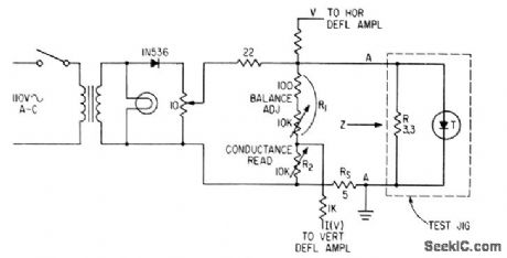
Positive half of 60-cps a-c voltage is applied to tunnel diode and to horizontal deflection amplifier of cro, and voltage across RS, proportional to diode current, is applied to vertical input. Arrangement gives display of complete characteristic throughout negative-resistance region.-J. A. Narud and T. A. Fyfe, Tunnel Diode Curve. Tracer is Stable in Negative Resistance Region, Electronics, 34:18, p 74-75. (View)
View full Circuit Diagram | Comments | Reading(973)
3_A_LOW_ROPOUT_REGULATOR_WITH_50_μA_QUIESCENT_CURRENT
Published:2009/7/16 20:51:00 Author:Jessie
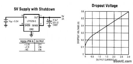
The LT1529 is a 3-A, 0.6-V dropout regulator with 50-μA no-load quiescent current and only 16 μA IQ shutdown. This makes the LT1529 useful for battery-powered applications where both long battery life and high-load current surges are expected. At 1.5-A load current, dropout voltage is just 0.43 V. The LT1529 needs no external diodes to protect against reverse battery or reverse output current faults. This allows the LT1529 to be used for backup power situations in which the output is held high while the input is at ground or reversed. (View)
View full Circuit Diagram | Comments | Reading(873)
13_V_SUPPLY
Published:2009/7/16 20:51:00 Author:Jessie
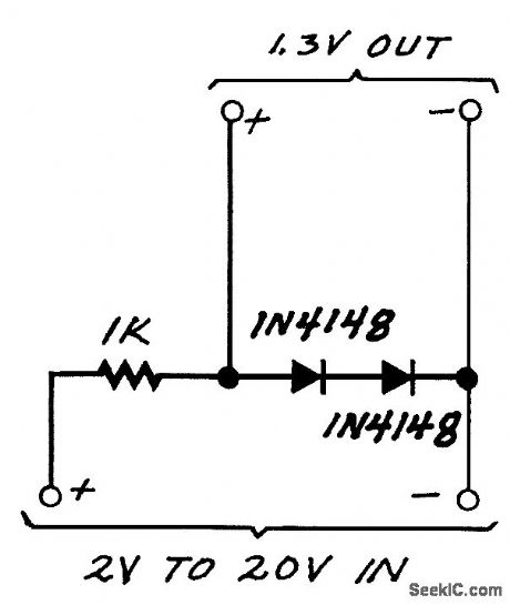
This s a simple 1.3-V regulator to power the ZN414IC. (View)
View full Circuit Diagram | Comments | Reading(740)
MINI_POWER_SOURCE
Published:2009/7/16 20:50:00 Author:Jessie
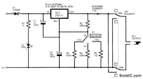
The figure shows a unit capable of offering different voltages to operate low-voltage appliances from a 12-V battery. Regulators of the LM317 type are current-limiting, short- circuit-proof, and over-heat-proof, although they are still not indestructible. This circuit will provide up to 1.5 A. IC1 should be heatsinked, perhaps by bolting it with an insulating kit to a metal box. (View)
View full Circuit Diagram | Comments | Reading(850)
FAST_DIFFERENTIAL_INPUT_CURRENT_SOURCE
Published:2009/7/16 20:50:00 Author:Jessie
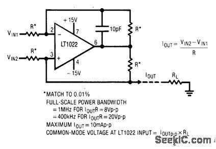
An LT1022 op amp used in this configuration can provide a rapidly switched current source. Use the equations in the figure to select component values. (View)
View full Circuit Diagram | Comments | Reading(873)
GASFET_POWER_SUPPLY
Published:2009/7/16 20:49:00 Author:Jessie
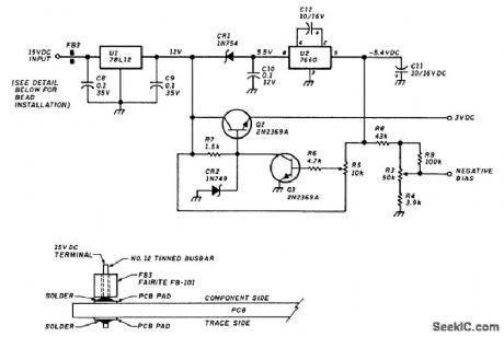
Suitable for use with the GASFET doubler In this text, and other similar applications, this supply delivers + 3 Vdc and 0 to -3 Vdc bias. (View)
View full Circuit Diagram | Comments | Reading(1123)
±15_V_FOR_SOUND_SYNTHESIZER
Published:2009/7/16 22:28:00 Author:Jessie
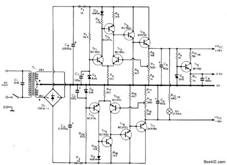
Provides highly stabilized voltages, required by elaborate sound synthesizer developed for generating wide variety of musical and other sounds. Circuit has additional 5-V output Tr6 requires heatsink dissipating 0.6 W, while heatsinks for Tr5 and Tr7 must each dissipate 14 W. Bridge rectifier is rated 100 V inverse peak at 2 A. Three-part article gives all circuits used in synthesizer.-T. Orr and D. W. Thomas, Electronic Sound Synthesizer, Wireless World, Part 3-Oct. 1973, p 485-490 (Part 1-Aug. 1973, p 366-372; Part 2 Sept.1973, p 429-434). (View)
View full Circuit Diagram | Comments | Reading(896)
SWITCHABLE_LINEAR_VOLTAGE_REGULATOR
Published:2009/7/16 22:27:00 Author:Jessie
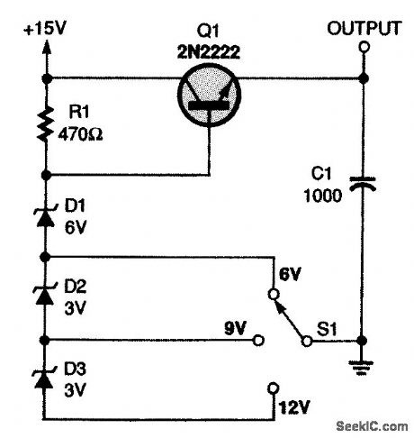
This three-voltage regulated supply can be added to for more voltage ranges. (View)
View full Circuit Diagram | Comments | Reading(805)
| Pages:84/291 At 2081828384858687888990919293949596979899100Under 20 |
Circuit Categories
power supply circuit
Amplifier Circuit
Basic Circuit
LED and Light Circuit
Sensor Circuit
Signal Processing
Electrical Equipment Circuit
Control Circuit
Remote Control Circuit
A/D-D/A Converter Circuit
Audio Circuit
Measuring and Test Circuit
Communication Circuit
Computer-Related Circuit
555 Circuit
Automotive Circuit
Repairing Circuit