
Circuit Diagram
Index 1413
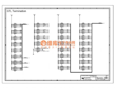
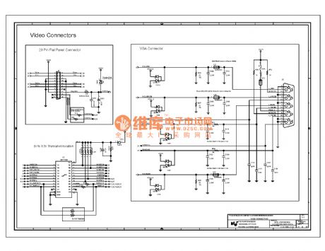
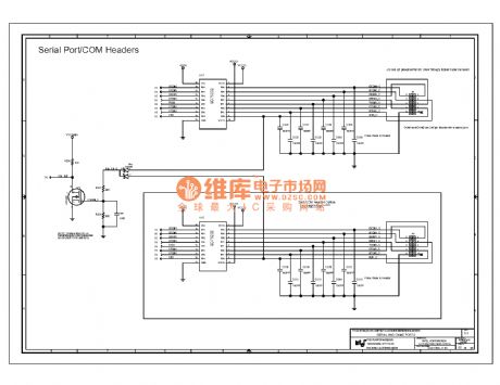
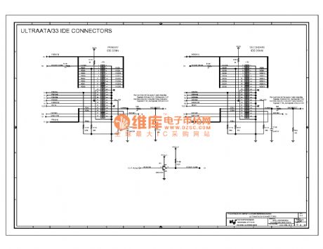
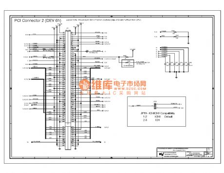
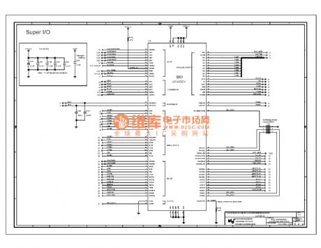
Computer motherboard circuit diagram 810 1_06
Published:2011/7/28 20:31:00 Author:Ecco | Keyword: Computer motherboard

View full Circuit Diagram | Comments | Reading(553)
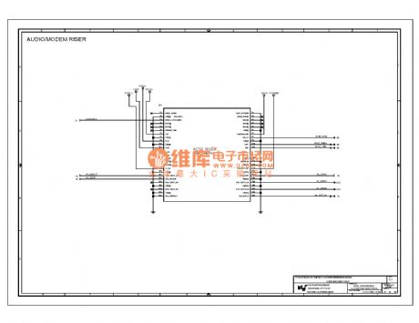
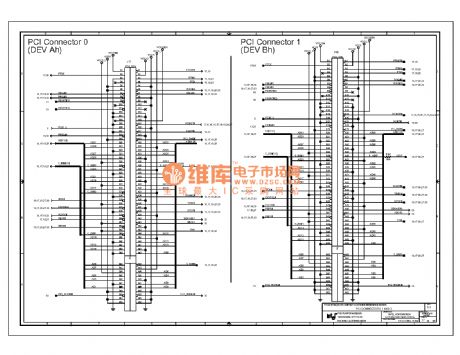
Computer motherboard circuit diagram 810 1_05
Published:2011/7/28 20:30:00 Author:Ecco | Keyword: Computer motherboard
View full Circuit Diagram | Comments | Reading(590)
PRECISION_CURRENT_SOURCE
Published:2009/6/18 23:29:00 Author:May
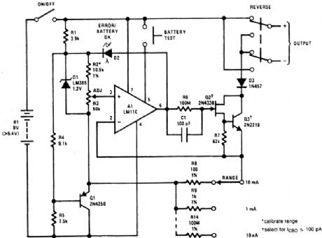
A complete, battery-powered current source suitable for laboratory use is shown. The op amp regulates the voltage acrosg the range resistors at a level determined by the voltage on the arm of the calibrated potentiometer, R3. The voltage on the range resistors is established by the current through Q2 and Q3, which is delivered to the output.The reference diode, D1, determines basic accuracy. Q1 is included to ensure that the LM11 inputs are kept within the common-mode range with diminishing battery voltage. A light-emitting diode, D2, is used to indicate output saturation. However, this indication cannot be relied upon for output-current settings below about 20 nA, unless the value of R6 is increased. The reason is that very low currents can be supplied to the range resistors through R6 without developing enough volt-age drop to turn on the diode.If the LED illuminates with the output open, there is sufficient battery voltage to operate the cir-cuit. But a battery test switch is also provided. It is connected to the base of the op-amp output stage and forces the output toward V+. (View)
View full Circuit Diagram | Comments | Reading(2370)
VARIABLE_VOLTAGE_ATTENUATOR
Published:2009/6/18 23:28:00 Author:May
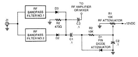
The front-end of this circuit is a bank of selectable bandpass filters. The output of the filter banks are shunted to ground via capacitor (C1) and PIN diode (D1). The PIN diode acts like an electroni-cally variable resistor. The resistance across the diode's terminals is a function of the applied bias voltage. This voltage, hence the degree of attenuation of the RE signal, is proportional to the setting of potentiometer RI. The series resistor (R2) is used to limit the current when the diode is forward biased. This step is necessary because the diode has a very low resistance when a certain rather low potential is exceeded. (View)
View full Circuit Diagram | Comments | Reading(864)
SQUARE_WAVE_OSCILLATOR
Published:2009/6/18 23:28:00 Author:May
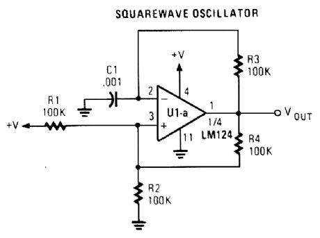
An Op amp with positive feedback generatesa square wave. The period ofthe oscillator is determined by R3 and C1.T=T1 + T2 ≈0.69×2 (R3C1) T1=T2 (View)
View full Circuit Diagram | Comments | Reading(1)
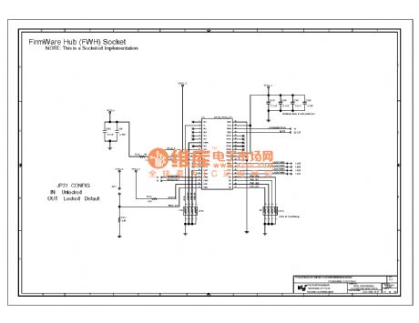
Computer motherboard circuit diagram 810 1_26
Published:2011/7/27 21:03:00 Author:Ecco | Keyword: Computer motherboard
View full Circuit Diagram | Comments | Reading(563)
Computer motherboard circuit diagram 810 1_25
Published:2011/7/27 21:03:00 Author:Ecco | Keyword: Computer motherboard
View full Circuit Diagram | Comments | Reading(579)
Computer motherboard circuit diagram 810 1_24
Published:2011/7/27 21:02:00 Author:Ecco | Keyword: Computer motherboard
View full Circuit Diagram | Comments | Reading(539)
Computer motherboard circuit diagram 810 1_23
Published:2011/7/27 21:02:00 Author:Ecco | Keyword: Computer motherboard
View full Circuit Diagram | Comments | Reading(559)
SWITCHABLE_POWER_ATTENUATOR
Published:2009/6/18 23:27:00 Author:May
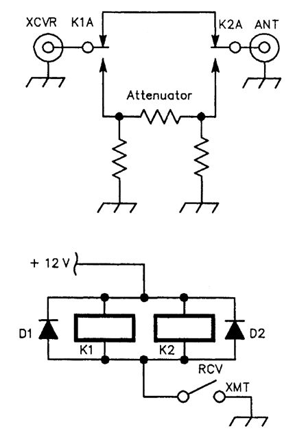
Schematic diagram of a switchable power attenuator that can be used to reduce the power output of transmitters that don't have ALC lines.
Values for 10 and 20 dB: 10 dB: R1 = R3 = 91 ΩR2 = 75 Ωnearest standard values 20 dB: R1 = R3 = 62Ω R2= 240 Ω nearest standard values
Note: R1 must handle the largest share of the input power, and R2 somewhat less. This depends on attenuation selected. (View)
View full Circuit Diagram | Comments | Reading(676)
Computer motherboard circuit diagram 810 1_22
Published:2011/7/27 21:01:00 Author:Ecco | Keyword: Computer motherboard
View full Circuit Diagram | Comments | Reading(550)
Computer motherboard circuit diagram 810 1_19
Published:2011/7/27 21:10:00 Author:Ecco | Keyword: Computer motherboard
View full Circuit Diagram | Comments | Reading(500)
Computer motherboard circuit diagram 810 1_18
Published:2011/7/27 21:10:00 Author:Ecco | Keyword: Computer motherboard
View full Circuit Diagram | Comments | Reading(550)
Computer motherboard circuit diagram 810 1_17
Published:2011/7/27 21:09:00 Author:Ecco | Keyword: Computer motherboard
View full Circuit Diagram | Comments | Reading(1164)
Computer motherboard circuit diagram 810 1_16
Published:2011/7/27 21:09:00 Author:Ecco | Keyword: Computer motherboard
View full Circuit Diagram | Comments | Reading(533)
Computer motherboard circuit diagram 810 1_15
Published:2011/7/27 21:09:00 Author:Ecco | Keyword: Computer motherboard
View full Circuit Diagram | Comments | Reading(676)
SIREN_OSCILLATOR
Published:2009/6/18 23:25:00 Author:May
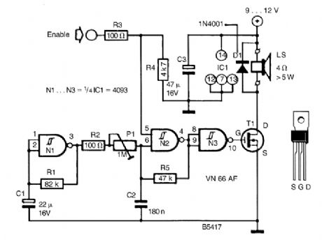
A CD4093 chip and a few components make up a siren oscillator, which drives power MOSFET T1. A 4-Ω speaker is driven directly from this device. The siren is enabled by a logic high applied to the ENABLE input. (View)
View full Circuit Diagram | Comments | Reading(3221)
ALTERNATE_TONE_ALARM
Published:2009/6/18 23:23:00 Author:May
A two-tone generator that is alternately switched ON provides a high/low output as might be heard from a traffic vehicle like a police car or ambulance.IC1, CD4011, quad 2-input NAND gate is a two-tone oscillator in which each side, pins 1 through 7 and 8 through 13 set the tone frequencies. Changing the values of C2 and C1 determines the high/low tones. The outout frequencies are coupled to IC2, CD4011, of which one side (pins 1 through 6) acts as a buffer. The buffer is necessary to prevent loading on the outputs that would occur if one tried to go directly to the LM386 amplifier. The other side of IC2, pins 8 through 13, is a slow pulse osciLator of approximately 8 Hz per second. The output at pin 10 is bonnected to IC4 as a clock.IC4, CD4027, is a dual J-K master-slave flip-flop that is wired to perform as a toggle switch in which Q1 and 15, and Q1 (NOT) pin 14, go high and low alternately (flip-flop). The clock input from IC2 pin 10 is connected to pin 13 of IC4, and the outputs at pins 15 and 14 changes the flip/flop state with each positive pulse transition. The CD4027 functions in toggle mode when the set and reset inputs, pins 9 and 12, are held low or grounded. Also, J-K inputs, pins 10 and 11, must be held high or to the positive.The outputs Q1 and Q1 (NOT), pins 15 and 14 are connected to pins 13 and 1 respectively oflC1 that enables or disables. Thus, each tone oscillator is turned on and off alternately. IC3 is a straightforward low-voltage audio amplifier. (View)
View full Circuit Diagram | Comments | Reading(1780)
ACTIVE_ANTENNA_FOR_UHF_SCANNERS
Published:2009/6/18 23:20:00 Author:May
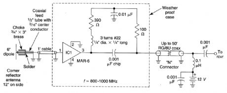
This active antenna IS a 1/2-wave dipole mounted In a 12"×12"×12"90°corner reflector,A builtin active preanlp IC1,fed dc through the RF coaxial line,provides 15 dB gain at 900 MHz to offset ca-ble losses,This provides supenor reception for scanners covering the 800- to 1000-MHz range. (View)
View full Circuit Diagram | Comments | Reading(717)
NEGATIVE_REFERENCE_VOLTAGE_CIRCUIT
Published:2009/6/18 23:19:00 Author:May
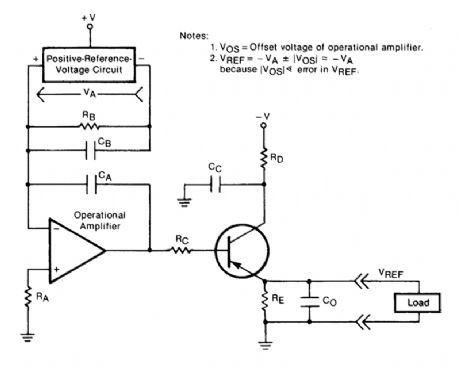
This figure illustrates a circuit that supplies a precise negative reference voltage. To meet requirements of accuracy and stability, it incorporates a highly precise positive reference voltage by use of a high-gain, stable feedback booster circuit.The booster circuit includes an operational amplifier and a transistor, which handles the load current. Typically, a po sitive-reference-voltage circuit can handle only relatively small load currents.This consideration does not apply in the present circuit because the p ositive-refer ence-voltage unit is placed in the voltage feedback loop of the booster circuit in parallel with resistor RB. Thus, from the perspective of the p o sitive-reference-v oltage unit,RB is a constant load. This feature enhances the stability of the circuit by removing the load regulation factor.Provided that the offset voltage of the operational amplifier is low, the accuracy of the overall circuit depends only on the accuracy of the p ositive-refer ence-voltag e unit. The overall circuit draws very little power for its own operation. It can handle unexpectedly heavy loads; the feedback conftg-uration and the high gain provided by the combination of the operational amplifier and the transistor give the circuit a very low output impedance. The capacitors reduce the noise voltage and help stabilize the circuit. In the event that the load becomes a short circuit, RD, protects the transistor by lim-iting the load current. (View)
View full Circuit Diagram | Comments | Reading(842)
| Pages:1413/2234 At 2014011402140314041405140614071408140914101411141214131414141514161417141814191420Under 20 |
Circuit Categories
power supply circuit
Amplifier Circuit
Basic Circuit
LED and Light Circuit
Sensor Circuit
Signal Processing
Electrical Equipment Circuit
Control Circuit
Remote Control Circuit
A/D-D/A Converter Circuit
Audio Circuit
Measuring and Test Circuit
Communication Circuit
Computer-Related Circuit
555 Circuit
Automotive Circuit
Repairing Circuit