
Circuit Diagram
Index 1407
OSCILLATOR_TRIGGERED_SWITCH
Published:2009/6/19 2:20:00 Author:May
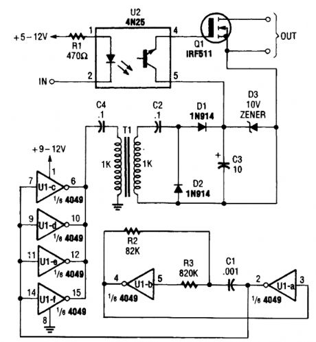
An oscillator is used here to generate a 9-V bias to switch Q1. This removes the need for a battery as a bias source. (View)
View full Circuit Diagram | Comments | Reading(1)
AUDIO_CONTROLLED_SWITCH
Published:2009/6/19 2:19:00 Author:May
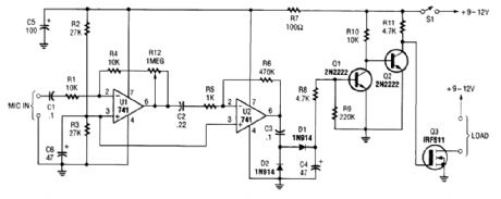
This audio-controlled switch combines a pair of 741 op amps, two 2N2222 general-purpose transistors, a hexFET, and a few support components to a circuit that can be used to turn on a tape recorder, a transmitter, or just about anything that uses sound. (View)
View full Circuit Diagram | Comments | Reading(0)
CIGRETTE_LIGHTER_9_V_ADAPTER
Published:2009/6/19 2:18:00 Author:May
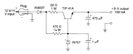
A simple way to provide +9 V at 100 mA from a 12-V auto source. Applications include small radios, cassettes, etc. (View)
View full Circuit Diagram | Comments | Reading(801)
DIGITAL_COMB_FILTER
Published:2009/6/19 2:18:00 Author:May
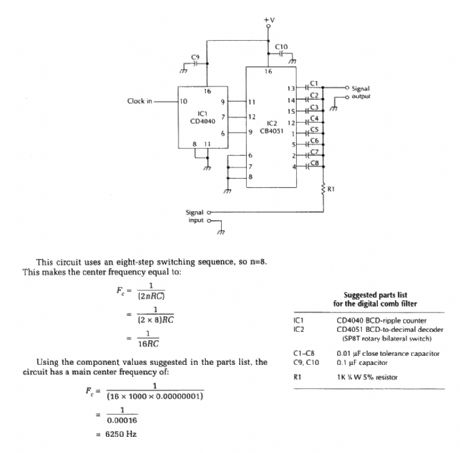
View full Circuit Diagram | Comments | Reading(918)
CAR_ALTERNATOR_MONITOR_IDIOT_LIGHT
Published:2009/6/19 2:17:00 Author:May
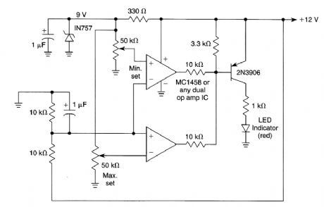
A window comparator is used to detect a too-low or a too-high system voltage. The minimum and maxirnum settings are set with two 50-kΩ pots, as desired. (View)
View full Circuit Diagram | Comments | Reading(2127)
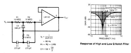
ADJUSTABLE_Q_NOTCH_FILTER
Published:2009/6/19 2:17:00 Author:May
This figure shows a circuit where the Q can be varied from 0.3 to 50. A fraction of the output is fed back to R3 and C3 by a second voltage follower, and the notch Q is dependent on the amount of signal fed back. A second follower is necessary to drive the twin T from a low-resistance source so that the notch frequency and depth will not change with the potentiometer setting. (View)
View full Circuit Diagram | Comments | Reading(0)
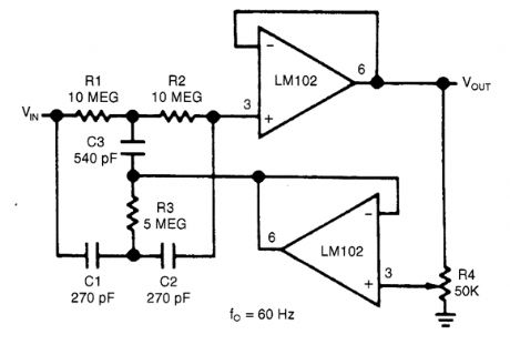
HIGH_Q_NOTCH_FILTER
Published:2009/6/19 2:16:00 Author:May
This shows a twin T network connected to an LM102 to form a high Q, 60-Hz notch filter. The Junction of R3 and C3: which is normally connected to ground, is bootstrapped to the output of the follower. Because the output of the follower is a very low impedance, neither the depth nor the frequency of the notch change; however, the Q is raised in proportion to the amount of signal fed back to R3 and C3. (View)
View full Circuit Diagram | Comments | Reading(0)
5G169 open-herding festival lantern larghing happily voice automatic control circuit
Published:2011/5/11 4:07:00 Author:May | Keyword: open-herding, festival lantern, larghing happily, voice automatic control
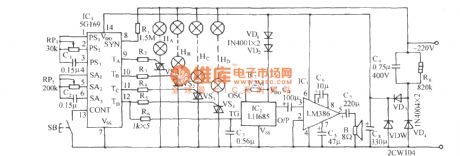
The circuit is shown in the diagram. It consists of starry carnival control circuit, laughter voice circuits, audio amplifier and rectifier voltage regulator, etc. (View)
View full Circuit Diagram | Comments | Reading(547)
ELECTRONIC_SAFETY_SWITCH
Published:2009/6/19 2:12:00 Author:May
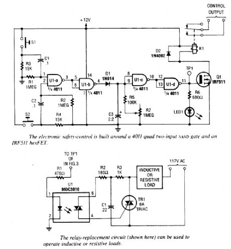
S1 and S2 must be depressed within 200 ms of each other to activate K1. The hold time is ad-justable via R7. S1 and S2 overlap time can be changed by changing C1 and C2 or R1 and R2. (View)
View full Circuit Diagram | Comments | Reading(701)
TRANSISTOR_MATCHING_CIRCUIT
Published:2009/6/19 2:11:00 Author:May
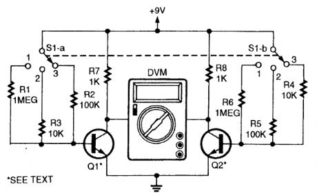
In order to match two transistors, select Q1 and Q2 so that they give zero readings(or as close as possible)on a DVM. The DVM acts as a null detector. An analog meter can be substituted. S1 should be set for an appropriate level of base current(approximately 8,80,or 800 μA). (View)
View full Circuit Diagram | Comments | Reading(1499)
EIGHT_CHANNEL_AUDIO_SWITCHER
Published:2009/6/19 2:10:00 Author:May
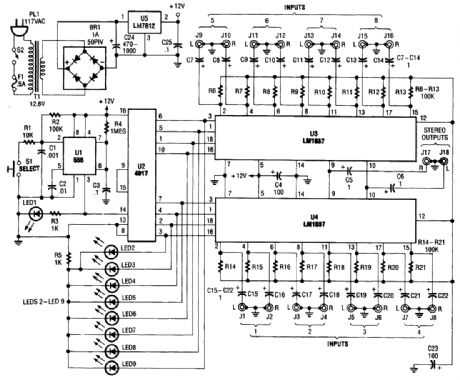
This source is selected by pressing momentary-contact pushbutton switch S1. Switch S1 is con-nected to the trigger of a 555 oscillator/timer (U1) configured as a monostable multivibrator, which generates one short output pulse for each press of S1. That pulse turns on LED1 to give a visible in-dication that the 555 is working correctly. That pulse is also used to clock U2 (a 4017 CMOS divide-by- 1 -counter/divider).Both LED1 and its associated current-limiting resistor R3 are optional and can be left out of the finished project without any affect on circuit operation. The 4017 advances by one clock pulse each time S1 is pressed, turning on its corresponding output. Pin 9 (corresponding to output 8) of U2 is directly connected to its own reset terminal at pin 15. This allows the counter to count from zero to seven, and then reset to zero on the eighth count.Pin 13, the enable input of U2, is tied to ground to allow the counter to operate. Outputs zero through seven are connected to eight indicator LEDs and the control pins of the two LM1037s (U3 and U4). When an output is selected, its LED lights and the corresponding control input on the LM1037 is brought high.The LM1037 has extremely high-impedance inputs and low-impedance outputs, so interconnec-tion between various types and brands of equipment should not be a problem. That, together with a wide-frequency response and low distortion, makes it ideal for use with good-quality, home-enter-tainment systems. The prototype of the audio switcher has a usable frequency response of from just a few hertz to over 100 kHz.Power for the switcher is provided by a rather simple circuit. Because the switcher only draws between 20 and 30 mA, a simple circuit using the popular 7812 or 78L12 (a low-power version) voltage regulator works quite well. (View)
View full Circuit Diagram | Comments | Reading(2913)
AUTOMOTIVE_ELECTRICAL_MONITOR
Published:2009/6/19 2:10:00 Author:May
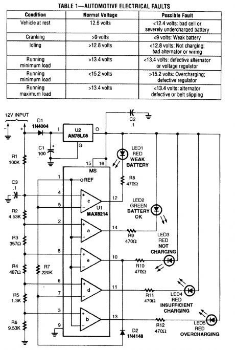
The automotive electrical diagnostic system is built around a Maxim MAX8214ACPE five-stage voltage comparator, which contains a built-in 1.25-volt precision reference, and on-board logic that allows the outputs of two of the comparators to be inverted. (View)
View full Circuit Diagram | Comments | Reading(875)
555 8kV high voltage generater circuit
Published:2011/5/11 4:10:00 Author:May | Keyword: 555, 8kV, high voltage generater
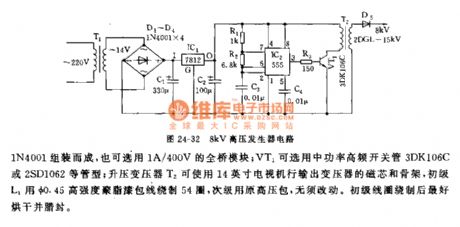
This high voltage generator can generate stable high voltage above 8kV. Its circuit is simple. It is stable and reliable. This circuit includes step-down rectifier, voltage regulator circuit, 18kHz multivibrator type oscillator and booster transformer, etc. Its circuit is shown in diagram 24-32.Step-down rectifier consists of step-down transformer T1 and full bridge rectifier and filter capacitor C1, etc. The rectified 15V DC voltage passes three terminal regulator 7812 to regulated voltage and outputted +12V stable DC voltage, it can offer working voltage for IC2, VT1, etc.Astable multivibrator consits of 555 and R1, R2, C3, etc. Its oscilating frenquency is fc=1.44/(R1+2R2)C3Parameter shown in diagram is designed according to 18.5kHz. (View)
View full Circuit Diagram | Comments | Reading(1799)
REFERENCE_CIRCUIT
Published:2009/6/19 2:09:00 Author:May
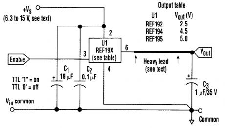
In this high-performance reference circuit, U1 is a device from the REF190 series producing de-vice-selectable outputs of 2.5, 4.5, and 5 V with simple, noncritical external circuitry. An Analog Devices REF 19 X(see the table in the figure)is used to derive a reference voltage. (View)
View full Circuit Diagram | Comments | Reading(996)
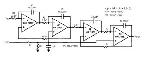
SINGLE_33_V_SUPPLY_4_POLE_STATE_VARIABLE_FILTER
Published:2009/6/19 2:09:00 Author:May
View full Circuit Diagram | Comments | Reading(632)
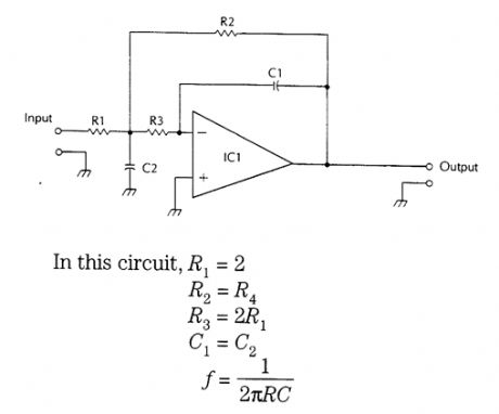
TWO_OP_AMP_BANDPASS_FILTER
Published:2009/6/19 2:08:00 Author:May


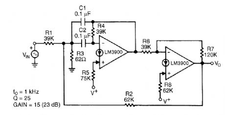
This circuit uses only two capacitors.The amplifier on the right supplies a controlled amount of characteristics. Resistors R5 and R8 are used to bias the outvoltage of the amplifiers at V+/2. (View)
View full Circuit Diagram | Comments | Reading(1)
ELECTRONIC_AUTO_STETHOSCOPE
Published:2009/6/19 2:06:00 Author:May
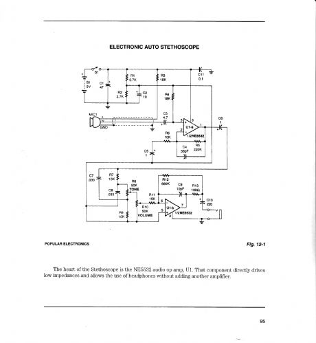
The heart of the Stethoscope is the NE5532 audio op amp, UI. That component directly drives low impedances and allows the use of headphones without adding another amplifier. (View)
View full Circuit Diagram | Comments | Reading(898)
ACTIVE_LOW_PASS_FILTER
Published:2009/6/19 2:04:00 Author:May
This circuit has a rolloff of 6 dB/Octave. (View)
View full Circuit Diagram | Comments | Reading(0)
555 AC voltage regulator delay and over-voltage alarm circuit
Published:2011/5/13 5:00:00 Author:May | Keyword: 555, AC voltage regulator, delay over-voltage alarm
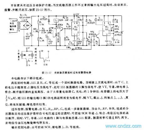
This set has the function of over voltage self protection. When AC voltage regulator works abnormally and output voltage is too high, it can realize automatic displaying, alarming and cutting off high voltage, as shown in diagram 21-17.
This circuit consists of high voltage delay circuit, over voltage detect, alarming circuit and output control circuit.
High voltage delay circuit: delay oscillation circuit consists of 555 and R7, C4, etc. When itis AC power supplied, the voltage on C4 can not break, pin 2 voltage is low level, meanwhile pin 3 of 555 oscillator is high level, it makes VT1 break over, relay Jo pulls in, DC high voltage of constant voltage source is cut off. Due to high capacity capacitor C4 charges, after about 1 minutes, voltage on capacitor is higher than 1/3Vdd, 555's output end (pin 3) changes to low level because circuit wraparound, and VT1 is cut off, Jo's touch spot Jo-1 and Jo-2 are reset, high voltage is turned on, red indicator is lit.
Over voltage detection, alarming circuit: multivibrator type oscillator consists of IC2, R10, RP2, C6, etc. When the voltage of over voltage protection signal thattaken out fromvoltage divider composed of R1, RP1 and R2 exceed given value, controlled silicon SCR breaks over, Jo is pull in, and it can cut off the high voltage of regulated power supply. At the same time, VT1 breaks over, pin 1 of 555 circuit is connected with power supply ground, 555 is Oscillating. Oscillating frequency can adjust by RP2. Sound signal sends out by piezoceramic buzzers.
Output control circuit: it consists of controlled silicon SCR, relay Jo, D7, etc. (View)
View full Circuit Diagram | Comments | Reading(2100)
PROGRAMMABLE_ANALOG_FILTER
Published:2009/6/19 2:03:00 Author:May
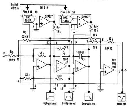
The circuit in the figure shows how an analog, digitally programmable filter can be built using a UAF42. This monolithic, state-variable active filter chip provides a two-pole filter building block with low sensitivity to extemal component variations. It eliminates aliasing errors and clock feed though noise common to switched-capacitor filters. Low-pass, high-pass, bandpass, and notch (band-reject) outputs are available. (View)
View full Circuit Diagram | Comments | Reading(1766)
| Pages:1407/2234 At 2014011402140314041405140614071408140914101411141214131414141514161417141814191420Under 20 |
Circuit Categories
power supply circuit
Amplifier Circuit
Basic Circuit
LED and Light Circuit
Sensor Circuit
Signal Processing
Electrical Equipment Circuit
Control Circuit
Remote Control Circuit
A/D-D/A Converter Circuit
Audio Circuit
Measuring and Test Circuit
Communication Circuit
Computer-Related Circuit
555 Circuit
Automotive Circuit
Repairing Circuit