
Circuit Diagram
Index 1406
dc_CONTROLLED_FET_SWITCH
Published:2009/6/19 2:28:00 Author:May
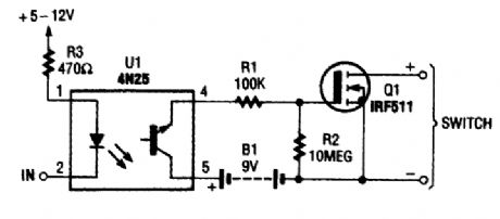
This dc-controlled switch uses an optoisolator/coupler, U1, to electrically isolate the input signal from the output-control device. (View)
View full Circuit Diagram | Comments | Reading(1564)
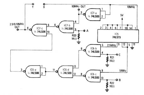
FREQUENCY_DIVIDER_FOR_10_MHz_FREQUENCY_STANDARD
Published:2009/6/19 2:28:00 Author:May
View full Circuit Diagram | Comments | Reading(886)
DC servo isolation amplifier circuit diagram
Published:2011/6/26 21:12:00 Author:Rebekka | Keyword: DC servo, isolation amplifier
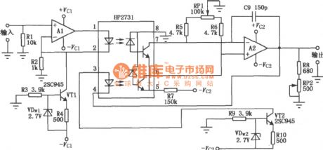
The picture shows the DC isolation servo amplifier circuit. When the analog signals are mixed with mode voltage noise, you can use this circuit to make the sensor input signals impend. In order to transmit the DC signal, the circuit uses servo means to form a feedback circuit to improve the stability of the circuit. A1 uses constant current drive optocoupler HP2731 in the light-emitting diode, the input signal bias current is 4mA. The optocoupler in the circuit uses double-type circuit HP2731. It has tracking performance. (View)
View full Circuit Diagram | Comments | Reading(2246)
74 Series digital circuit 74376 four J-K non-flip-flop
Published:2011/5/13 5:02:00 Author:May | Keyword: digital, four J-K, non-flip-flop
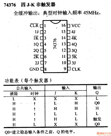
74376 four J-K non-triggerfull buffer output: typical clock input frequency is 45MHz
(View)
View full Circuit Diagram | Comments | Reading(850)
VSB_FILTER_FOR_LM2889
Published:2009/6/19 2:27:00 Author:May
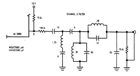
This filter is for CH3, in order to get a vestigial sideband TV signal. It is designed for 75-Ω im-pedance levels. (View)
View full Circuit Diagram | Comments | Reading(770)
74 Series digital circuit 74S340 74S341 and other eight buffer/line driver (three-state)
Published:2011/5/11 3:57:00 Author:May | Keyword: digital, eight buffer, line driver, three-state
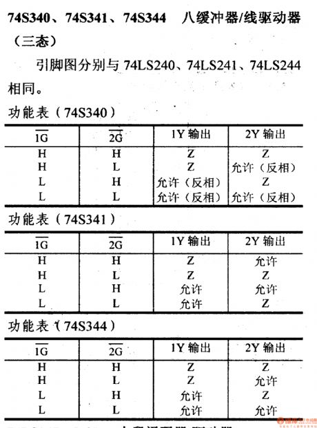
74S340, 74S341, 74S344 eight buffer/line driver (tristate)Their pin diagrams is seperately same as 74LS240, 74LS241, 74LS244.
(View)
View full Circuit Diagram | Comments | Reading(637)
HEXFET_SWITCH
Published:2009/6/19 2:27:00 Author:May
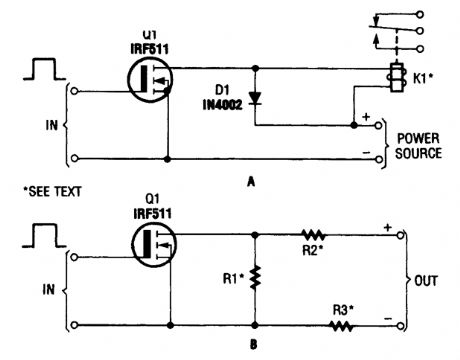
The hexFET can switch dc power to relays (as shown in A), motors, lamps, and numerous other devices. That arrangement can even be used to switch resistors in and out of a circuit, as shown in B. R1, R2, and R3 represent resistive loads that can be switched in and out of the circuit. (View)
View full Circuit Diagram | Comments | Reading(1121)
VOLTAGE_CONTROLLED_LOW_PASS_FILTER
Published:2009/6/19 2:26:00 Author:May
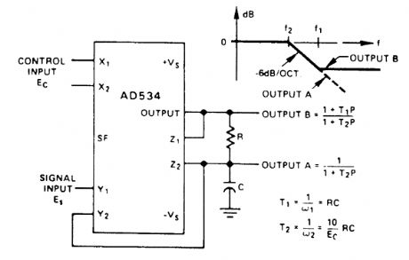
The voltage at Output A, which should be unloaded by a follower, responds as though ES were di-rected to the RC filter, but the filter's break frequency were proportional to Ec[i.e,.=Ec/(20πRC)] The frequency response has a break at f2; and the 6-dB/octave rolloff. The voltage at Output B has the same response, up to [f1 (f = 1/(20πRC)], then levels off at a constant attenuation of f2/f1 = Ec\10.For example, if R = 8kΩ, C = 0.002μF, Output A has a pole at 100 Hz to 10 kHz and can be loaded.The circuit can be converted to high-pass by interchanging C and R. (View)
View full Circuit Diagram | Comments | Reading(1)
TURN_SIGNAL_ALARM
Published:2009/6/19 2:25:00 Author:May
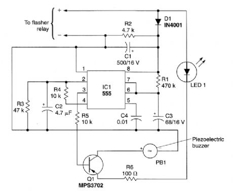
This circuit can be used to tell the driver of a vehicle when his or her turn signal has been left on for too long. The circuit consists of IC1, a 555 timer; transistor Q1, and MPS3702 PNP preamp/driver; PB1, a piezoelectric buzzer; along with an assortment of resistors, capacitors, and diodes. The 555 is connected in the mono.stable mode, requiring only a momentary negative pulse at pin 2 to trigger the timing cycle.Power for the circuit is picked off the flasher relay and applied to IC1, pin 8, provided by an ini-tially discharged capacitor, C2. After the initial triggering, the voltage across C2 rises as it becomes charged through R4, a 10-kΩ resistor. This prevents subsequent interference with the delay function caused by false triggering.Capacitor C3 and resistor R1 determine the delay. With the component values shown, a delay of about one minute will be provided before the intermittent tweet sound generated by the circuit be-gins. If higher values are used for C2 and R1, a longer delay time will result. The light-emitting diode, LED1, provides a voltage drop to assure complete transistor blocking during the off periods of the flasher. Alternatively, two diodes in series can be used. (View)
View full Circuit Diagram | Comments | Reading(1803)
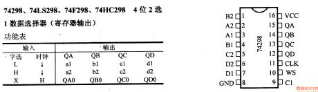
74 Series digital circuit 74298 74LS298 and other 4-bit 2 selects 1 data selector (register output)
Published:2011/5/11 3:58:00 Author:May | Keyword: digital, 4-bit, 2 selection 1, data selector, register output
View full Circuit Diagram | Comments | Reading(1142)
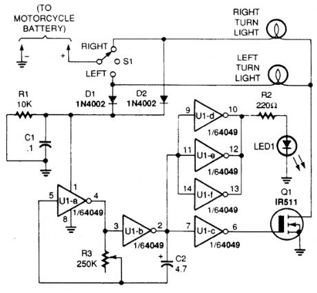
SMART_TURN_SIGNAL_FOR_AUTOS_AND_MOTORCYCLES
Published:2009/6/19 2:24:00 Author:May
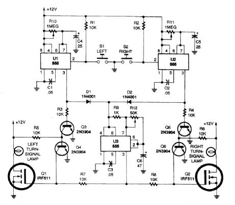
Momentarily pressing S1 starts the left on-time timer and produces a positive output at pin 3 of U1. Power for the on/off signal timer, U3, is supplied through D1.Also, a positive bias is supplied from U1's output to the base of Q3, turning it on and turning Q4 off. Unclamped Q1 turns the left turn-signal lamp on and off at that same low-frequency rate. Because U2 is not activated, its output at pin 3 is low, keeping Q5 off. With Q5 turned off, Q6 is on, clamping the gate of Q2 to ground and keeping it from responding and supplying an output for the right turn-signal lamp. The left turn signal continues to operate until the UI timer circuit times out; the right turn signal operates in a similar manner, with U2 setting its operating time.Potentiometer R10 sets the running time for the left turn signal and R11 sets that for the right turn signal. (View)
View full Circuit Diagram | Comments | Reading(699)
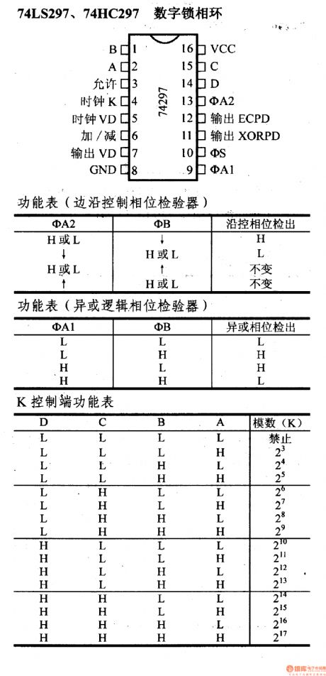
74 series digital circuit 74LS297 74HC297 and other digital phase-locked loop
Published:2011/5/11 3:59:00 Author:May | Keyword: digital, digital phase-locked loop
View full Circuit Diagram | Comments | Reading(1102)
TYPICAL_TWO_WAY_SWITCH_WIRING
Published:2009/6/19 2:23:00 Author:May
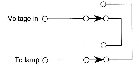
When the light is off, it can be turned on with either switch. When it's on, it can be turned off with either switch. (View)
View full Circuit Diagram | Comments | Reading(784)
74 series digital circuit 74166 74LS166 and other eight bits shift registers (serial/parallel-serial out)
Published:2011/5/11 3:59:00 Author:May | Keyword: digital, eight bits, shift register, serial/serial/parallel out
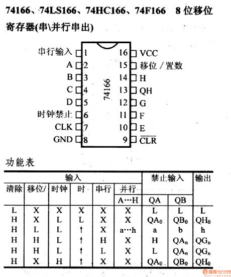
View full Circuit Diagram | Comments | Reading(3208)
AUTO_RANGING_DIGITAL_CAPACITANCE_METER
Published:2009/6/19 2:23:00 Author:May
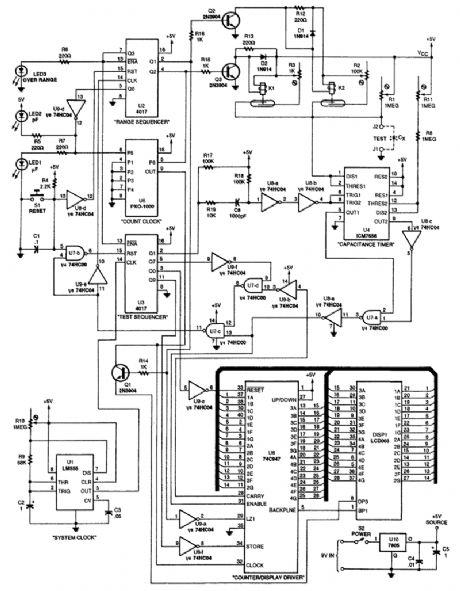
This digital capacitance meter reads from 1 pF to 1000 μF. Basically, a timer(U4)uses the unknown capacitance to generate a pulse of duration, depending on the value of unknown capacitance, and the pulse duration is measured. The display is an LCD 0003 driven by a 74C947 counter/display driver. (View)
View full Circuit Diagram | Comments | Reading(1675)
Incandescent lamp life extension switch circuit 2
Published:2011/5/11 4:02:00 Author:May | Keyword: Incandescent lamp, life extension, switch
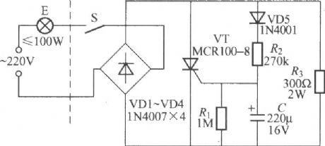
The diagram is shown in the diagram. Right hand of broken line in the diagram is life extension switch, left is ordinary light circuit, so lamp E and switch adopt two lines connection, namely single line input and output, it can directly replace ordinarily switch and does not need to change the original cabling indoor. (View)
View full Circuit Diagram | Comments | Reading(1467)
LOAD_DISCONNECT_SWITCH
Published:2009/6/19 2:22:00 Author:May
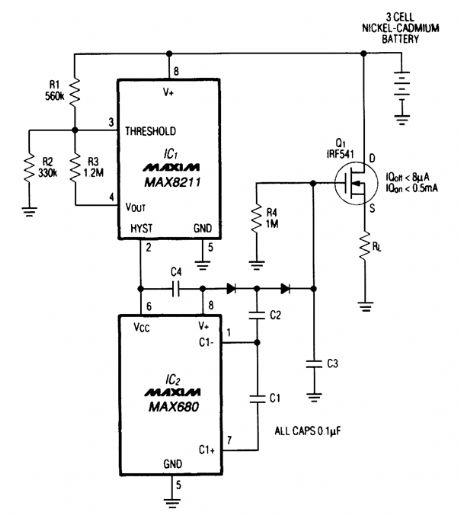
Deep discharge can damage a rechargeable battery. By disconnecting the battery from its load, this circuit halts battery discharge at a predetermined level of declining terminal voltage. Transistor Q1 acts as the switch. The overall circuit draws about 500 μA when the switch is closed and about 8 μA when the switch is open. (View)
View full Circuit Diagram | Comments | Reading(1238)
TACHOMETER_SIGNAL_CONDITIONING_CIRCUIT
Published:2009/6/19 2:21:00 Author:May
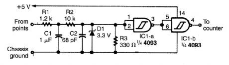
This circuit, for use with auto tachometers, cleans up the ragged distribution waveform before it is sent to pulse counter circuits. (View)
View full Circuit Diagram | Comments | Reading(980)
CS7232 touch-free dimming light circuit 1
Published:2011/5/11 4:05:00 Author:May | Keyword: touch-free, dimming light
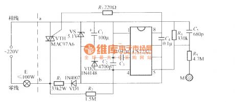
The diagram shows touch-free dimming light made of CS7232 dimming application specific integrated circuit. Touch M can adjust the light of lamp E with none stage. (View)
View full Circuit Diagram | Comments | Reading(1000)
MOTORCYCLE_TURN_SIGNAL_SYSTEM
Published:2009/6/19 2:20:00 Author:May
Tired of making hand signals? Build this simple turn-signal system and keep your hands on the handlebars. (View)
View full Circuit Diagram | Comments | Reading(140)
| Pages:1406/2234 At 2014011402140314041405140614071408140914101411141214131414141514161417141814191420Under 20 |
Circuit Categories
power supply circuit
Amplifier Circuit
Basic Circuit
LED and Light Circuit
Sensor Circuit
Signal Processing
Electrical Equipment Circuit
Control Circuit
Remote Control Circuit
A/D-D/A Converter Circuit
Audio Circuit
Measuring and Test Circuit
Communication Circuit
Computer-Related Circuit
555 Circuit
Automotive Circuit
Repairing Circuit