
Circuit Diagram
Index 1418
VACUUM_TUBE_LOW_POWER_80_40_METER_TRANSMITTER
Published:2009/6/18 5:12:00 Author:May
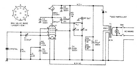
Using a 6BW6 vacuum tube, the above transmitter delivers about 5 W output. C1 is adjusted for cleanest CW note. C8 and C9 are 365 pF and dual-365 pF (paralleled) tuning capacitors. L1 is 35 turns of #24 enamelled wire on a 1 plastic tube. FT-243 crystals for 3.5 or 7-MHz are used. Do not use this circuit to produce a 7-MHz output from a 3.5-MHz crystal-it is not intended to double over crystal frequencies. (View)
View full Circuit Diagram | Comments | Reading(2816)
LOW_COST_ACCURATE_SQUARING_CIRCUIT
Published:2009/6/18 5:12:00 Author:May
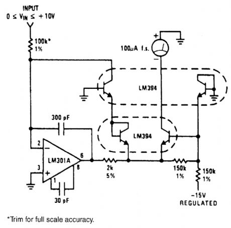
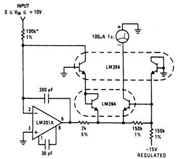
The circuit shown will square the input signal and deliver the result as an output current.Full-scale input is 10V,but this can be changed simply by changing the value of the 100-kQ input resis-tor.As in the square root Gircuit, the -15-V supply is used as the reference. In this case, however, a 1% shift in supply voltage produces a 1% shift in the output signal.The 150-kQ resistor across the base-emitter of 1/2LM394 provides slight temperature compensation of the reference current from the -15-V supply.For improved accuracy at low input signal levels,the offset voltage of the LM301A should be zeroed out,and a 100-kQ resistor should be inserted in the positive input to provide input to provide optimum dc balance. (View)
View full Circuit Diagram | Comments | Reading(843)
SIMPLE_FM_TRANSMITTER
Published:2009/6/18 5:08:00 Author:May
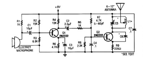
Running from a 9-V battery, this transmitter can be used as a wireless rrticrophone with an ordi-nary 88- to 108-MHz FM broadcast receiver. Keep the antenna length under 12 inches to comply with FCC limits. L1 is 6 tums of #24 wire wound around a pencil or a 1/4 form, with tums spaced I wire diameter. C6 is a gimmick capacitor of about 1 pF. (View)
View full Circuit Diagram | Comments | Reading(682)
6_W_ECONOMY_MORSE_CODE_TRANSMITTER_FOR_7_MHz
Published:2009/6/18 5:06:00 Author:May
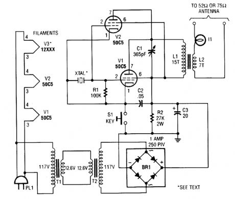
The vacuum tube is still alive and useful in some applications, as in this CW transmitter. The circuit was built in old-fashioned breadboard style on a wooden base. Old table radios are a good source of parts for this circuit. V3 is used as a ballast resistor-a 75-Ω, or 100-Ω 5-W resistor could be sub-stituted. L1 is 15 turns of hookup wire on a 7/8 form 2 long. L2 is 7 turns of the same wire. L2 is wound over L1. Be careful as up to 160 V is present on VI and V2. (View)
View full Circuit Diagram | Comments | Reading(1607)
ATV_DOWNCONVERTER_FOR_420_TO_450_MHz
Published:2009/6/18 5:02:00 Author:May
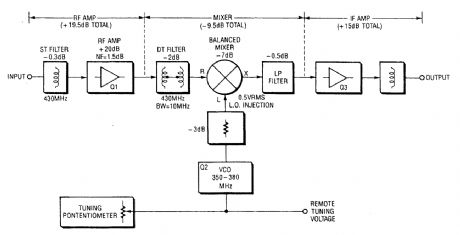
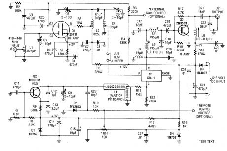
This ATV downconverter converts the 420- to 450-MHz ATV band, which is several channels be-tow the lower limit of the UHF band, to channel 3 or 4 for viewing on virtually any TV. The down-converter has a low-noise preamplifier stage and a double-balanced passive mixer for good performance and a wide dynamic range. That is necessary with today's crowded UHF bands. The converter draws about 27 milliamperes from a 13.2-volt dc source, so it can be used in portable and mobile applications. An extra IF stage gives an overall gain of about 25 dB. A block diagram of the clownconverter is also shown. A complete kit of parts, including PC board, is available from North Country Radio, P.O. Box 53, Wykagyl Station, New Rochelle, NY 10804-0053A. (View)
View full Circuit Diagram | Comments | Reading(2007)
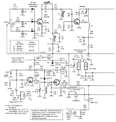
ATV_JR_TRANSMITTER_440_MHz
Published:2009/6/18 5:00:00 Author:May
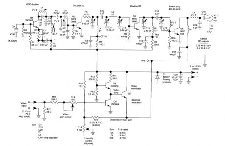
This low-power video transmitter is useful for R/C applications, surveillance, or amateur radio applications. Seven transistors are used in a crystal oscillator multiplier RF power amplifier chain, and a high-level video modulator. A 9-to 14-Vdc supply is required. Output is 0.4 to 1.2 W, depending on supply voltage. A complete kit of parts is available from North Country Radio, P.O.Box 53, Wykagyl Station, NewRochelle, NY 10804-00530 (View)
View full Circuit Diagram | Comments | Reading(4639)
VERY_EFFICIENT_SOLENOID_DRIVER
Published:2009/6/18 4:59:00 Author:May

In the circuit shown, the IC in the center, U1, contains a microprocessor-compatib le serial-in, parallel-out shift register, with strobed latch and high-level solenoid drives (see the figure).The strobe pulse turns on the selected loads at full power for its pulse width, which is 0.5 sec-ond. Following the strobe pulse, the driver outputs are pulse-width modulated by the multivibrator, which is set for a duty cycle of 25%. The solenoids are therefore held in the engaged position with a voltage that's 25% of the nominal supply voltage.U2B acts as the basic multivibrator in the circuit, and U2A sets the duty cycle by setting the dis-charge current of capacitor C1. U2D overrides the oscillation during the strobe pulse. And U2C pro-vides the Power-On Reset (POR), inhibiting the solenoid loads from turning on during the initialization period of the microprocessor. (View)
View full Circuit Diagram | Comments | Reading(1386)
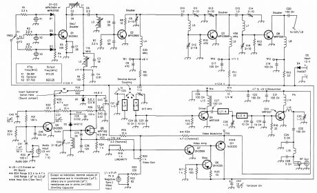
THREE_CHANNEL_420_TO_450_MHz_ATV_TRANSMITTER
Published:2009/6/18 4:59:00 Author:May
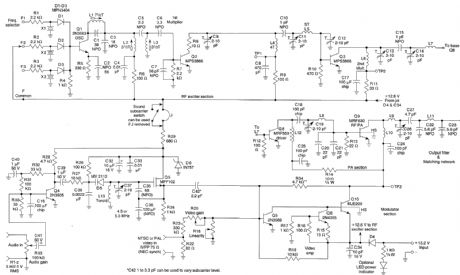
This transmitter is a 2-watt PEP output device for 420- to 450-MHz amateur TV operation. It has three crystal-controlled channels and will accept standard NTSC video input. It also has a 4.5-MHz sound subcarrier capability. Because this transmitter has AM modulation, audio can be transmitted in AM form on the RE carrier by applying audio to the video input. Bandwidth of audio can be restricted to 20 kHz by placing a 0.002-pF capacitor across R34. A complete kit of parts, including PC board is available from North Country Radio, P.O. Box 53, Wykagyl Station, New Rochelle, NY 10804-0053A. (View)
View full Circuit Diagram | Comments | Reading(2032)
ULTRA_LOW_DISTORTION±50_mA_DRIVER
Published:2009/6/18 4:57:00 Author:May
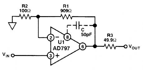
For a 600-Ω load,THD is typically-115 dB at 20 kHz,3-V RMS output,、with±15-V supplies The-3-dB BW is 6 MHz. (View)
View full Circuit Diagram | Comments | Reading(844)
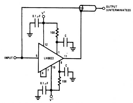
COAX_CABLE_DRIVER
Published:2009/6/18 4:56:00 Author:May
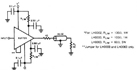
Becbuse of their high-current drive capability, the LH0002, LH0033, and LH0063 buffer ampli-fiers are suitable for driving terminated or unterminated coaxial cables, and high-current or reactive loads. Current-limiting resistors should be used to protect the device from excessive peak load cur-rents or accidental short circuit. No current limiting is built into the devices other than that imposed by the limited beta of the output transistors. This figure shows a coaxial-cable drive circuit. The 43-Ω resistor is included, the output voltage to the load is about half what it would be without the near-end termination. (View)
View full Circuit Diagram | Comments | Reading(1387)
VIDEO_CABLE_DRIVER
Published:2009/6/18 4:55:00 Author:May
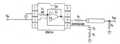
The driver's frequency response is tunable for a specific cable length via components connected to the summing node. By shunting R1,RC, acts to increase the amplifier's gain, and CC controls the cut-in frequency of the compensation.These three components peak the amplifier's frequency response to counteract the cable's roll-off characteristic. By squeezing more bandwidth out of a given cable, higher-performance cables aren't needed. (View)
View full Circuit Diagram | Comments | Reading(0)
LOW_DISTORTION_COMPOSITE±100_mA_LINE_DRIVER
Published:2009/6/18 4:54:00 Author:May
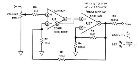
This line driver combines the high input impedance of an FET-input IC and a 100-mA op amp.U1's output is left open. The compensation terminal (pins) drive U2's high-Z input for increased overall phase margin. Gain is 14 dB, THD +N at 5 V, and RMS output is around 0.001% below 20 kHz. (View)
View full Circuit Diagram | Comments | Reading(1150)
TTL_BASED_SPEAKER_DRIVER
Published:2009/6/18 4:52:00 Author:May
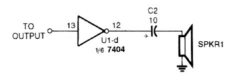
A TTL IC, such as a 7404, can drive a small speaker with enough audio to be used as an alarm or annunciator. The speaker can be a 32- or 100-Ω unit. (View)
View full Circuit Diagram | Comments | Reading(1073)
HIGH_SIDE_MOSFET_DRIVER
Published:2009/6/18 4:51:00 Author:May
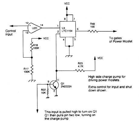
A Linear Technology LTC1154 is used as a charge pump to drive the gate of a high-side power MOSFET. (View)
View full Circuit Diagram | Comments | Reading(1381)
ATV_DOWNCONVERTER_FOR_902_TO_928_MHz
Published:2009/6/18 4:51:00 Author:May
This clownconverter converts ATV signals in the 902- to 928-MHz range to a 61.26- or 67.25-MHz IF output frequency (CH 3 or CH 4) to enable reception of these signals on a standard VHF TV receiver or monitor. It features a low-noise RF amp feeding a Schottky diode double-balanced mixer, a tunable LO and one IF preamp stage. The RF amplifier is a low-noise dual-gate GASFET that is followed by a sec-ond RE stage using an MMIC. Five tuned circuits are used in the RE amplifier. This feeds a packaged Schottlqr diode mixer assembly for better dynamic range and reduced susceptibility to intermodulation and strong signal areas. The on-board local oscillator (LO) is voltage tuned and if desired can be set up for remote tuning. Ail necessary circuitry for remote tuning is on board for coax dc and IF feed. This enables the clownconverter to be mast mounted to get around feedline losses generally associated with this frequency range. No separate dc feed is necessary because the coax (RG59/U recommended) carries dc power, tuning voltage, and IF signal. A dc block is used at the receiver for the purpose of separating dc voltage supply and the tuningvoltage. This allows a cable run of several hundred feet, if needed.By using this clownconverter and transmitter, a physically small915-MHz ATV station or even a video HT can be constructed because both units are each 2.50 x 4.00 inches x 1.00 high, and can be stacked together. A complete kit of parts, including PC board is available from North Country Radio, P.O. Box 53, Wykagyl Station, New Rochelle, NY 10804-0053A. (View)
View full Circuit Diagram | Comments | Reading(1479)
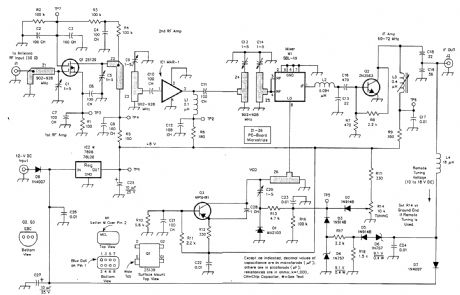
10_M_DSB_QRP_TRANSMITTER_WITH_VFO
Published:2009/6/18 4:48:00 Author:May
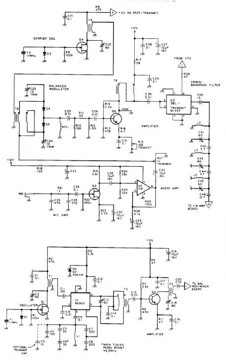
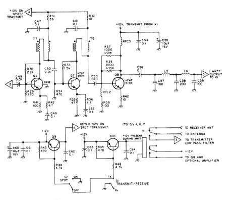
The three schematics represent three building blocks for a 10-meter SSB transmitter. Or these blocks can be used separately as circuit modules for other transmitters. The VFO board uses an FET transmittal oscillator, the VFO signal is mixed in an NE602 mixer and is amplified by Q2 to a level suf-ficient to drive an SBL-1 mixer in the transmit mixer stage (+7 to +10 dBm). In the balance mixer/modulator board, an 11-MHz crystal oscillator drives a diode balanced mixer. Audio for mod-ulation purposes is also fed to this mixer. The DSB signal feeds a 28-MHz BPR The 1-W amplifier board consists of a 3-stage amplifier and transmit/receive switching circuitry. (View)
View full Circuit Diagram | Comments | Reading(10129)
SIMPLE_NEON_LIGHT_DRIVER
Published:2009/6/18 4:44:00 Author:May
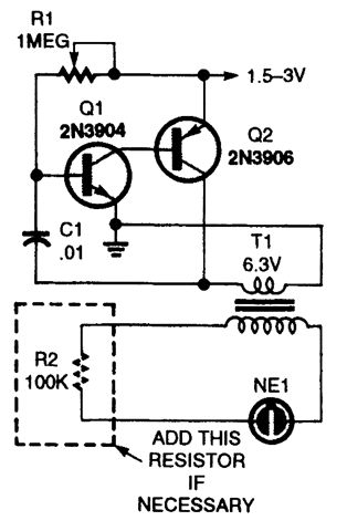
NE1, a neon lamp, is lit by this simple inverter circuit. T1 is a 20:1 tum ratio transformer (transistor radio output, etc.). (View)
View full Circuit Diagram | Comments | Reading(1733)
27125_MHz_NBFM_TRANSMITTER
Published:2009/6/18 4:44:00 Author:May
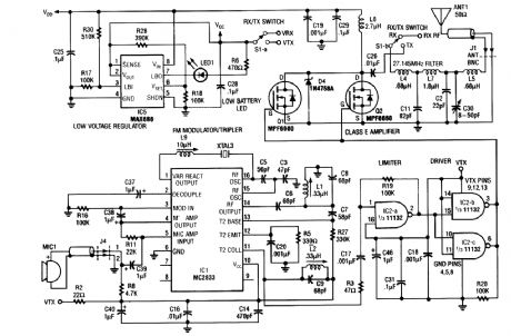
Using a Motorola MC2833 one-chip FM transmitter, a few support components, and an MPF6660 FET RF amp, this trans-mitter delivers about 3 W into a 50-Ω load. It is capable of operation over about 29 to 32 MHz with the components shown. (View)
View full Circuit Diagram | Comments | Reading(1537)
HIGH_SPEED_SHIELD_LINE_DRIVER
Published:2009/6/18 4:42:00 Author:May
View full Circuit Diagram | Comments | Reading(715)
THREE_CHANNEL_902_TO_928_MHz_ATV_TRANSMITTER
Published:2009/6/18 4:42:00 Author:May
This transmitter is for ATV applications in the 902- to 928-MHz band. It has three crystal-con-trolled channels, and will accept standard NTSC video input. It also has a 4.5-MHz sound subcarrier.Because this is an lNI transmitter, audio can be transmitted as AM on the RF carrier. Simply use the video input Bandwidth。f audio can be restricted to dU kHz by placing a capacitor with a value of about o.002 pF across R34 The output is 1 5 to 2 watts PEP into a 50-Ω load,A complete kit of partsincluding PC board,is available from North Country Radio,P.O 0.Box 53,Wyktation,New Rochelle,NY 10804-0053A (View)
View full Circuit Diagram | Comments | Reading(1826)
| Pages:1418/2234 At 2014011402140314041405140614071408140914101411141214131414141514161417141814191420Under 20 |
Circuit Categories
power supply circuit
Amplifier Circuit
Basic Circuit
LED and Light Circuit
Sensor Circuit
Signal Processing
Electrical Equipment Circuit
Control Circuit
Remote Control Circuit
A/D-D/A Converter Circuit
Audio Circuit
Measuring and Test Circuit
Communication Circuit
Computer-Related Circuit
555 Circuit
Automotive Circuit
Repairing Circuit