
Circuit Diagram
Index 1416
VOICE_ACTIVATED_SWITCH_AND_AMPLIFIER
Published:2009/6/18 22:31:00 Author:May
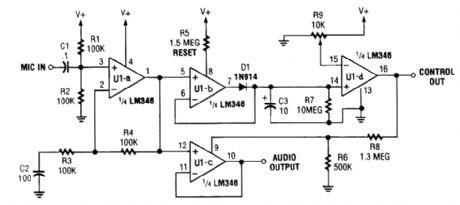
In certain applications, such as transmitter or other communications and control applications, this circuit should be useful. Both audio output and dc control outputs are provided. R9 sets the con-trol threshold. (View)
View full Circuit Diagram | Comments | Reading(1757)
REMOTELY_POWERED_SENSOR_AMPLIFIER
Published:2009/6/18 22:31:00 Author:May
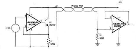
For rerrtote sensor applications, this circuit enables use of a single twisted pair. (View)
View full Circuit Diagram | Comments | Reading(1148)
PROGRAMMABLE_INPUT_AMPLIFIER
Published:2009/6/18 22:30:00 Author:May
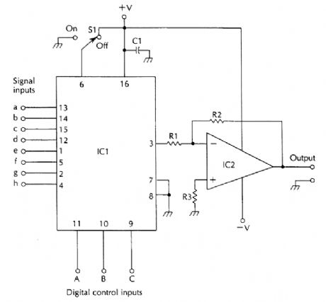
This amplifier has eight inputs selectable digitally.
IC1 CD4051 SP8T bilateral switch R1 10-kΩ 1/4-W 5% resistorIC2 Op amp to suit application R2 22-kΩ 1/4-W 5% resistorC1 0.1-μF capacitor R3 18-kΩ 1/4-W 5% resistorS1 SPST switch (View)
View full Circuit Diagram | Comments | Reading(1576)
AUDIO_LIGHT
Published:2009/6/18 22:30:00 Author:May
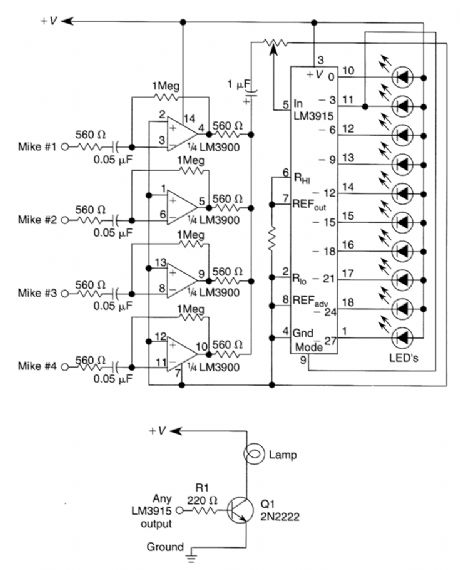
This circuit will produce an output when the sound exceeds a preset level. The LM3915 is a log-output bar graph driver. Use the transistor driver shown for higher current loads. To drive heavy-current loads with an LM3915 output, you must add a transistor, as shown in B. (View)
View full Circuit Diagram | Comments | Reading(2478)
WHISTLE_SWITCH
Published:2009/6/18 22:29:00 Author:May
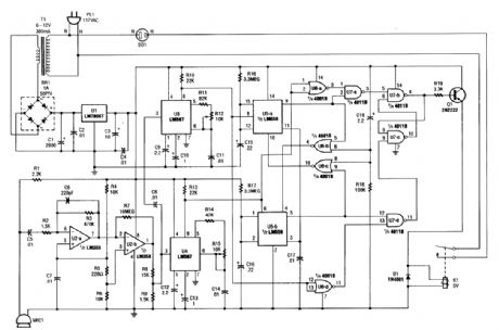
At the heart of the whistle switch are a pair of tone detectors, each of which is built around an LM567 tone decoder, which are supported by a ntinimum of additional components. This whistle switch is designed to respond to only two or more occur-rences of a specific tone, or sequence of tones, within a specified period to prevent false triggering. Depending on the relay used, various ac loads can be controlled. Microphone MIC1 picks up the sound and U2 amplifies the signal and feeds it to tone decoders U3 and U4. These devices trigger U5-a and U5-b and the logic circuits that drive relay K1. (View)
View full Circuit Diagram | Comments | Reading(2056)
VOICE_IDENTIFIER_FOR_HAM_RADIO_USE
Published:2009/6/18 22:27:00 Author:May
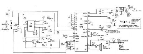
Using an ISD1016 audio record/playback chip (Information Storage Devices, Inc.), this circuit records and plays back mes-sages on command. Although intended for use with transmitters, it can be used as an electronic notepad, etc. Consult the ISD1016 data sheet for other applications. (View)
View full Circuit Diagram | Comments | Reading(2617)
AUTOMATIC_FADER
Published:2009/6/18 22:25:00 Author:May
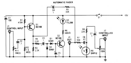
In this circuit, audio fed to the control channel is amplified and rectified by D1 and D2. This dc level activates LED D3 via Q2. The light from D3 causes R9, a light-dependent resistor to decrease resistance. As R11 (audio gain) is set higher, more audio is present at the output of Q1. Audio fed into J2 is shunted to ground via R9 and less of this audio appears at J3. Therefore, audio at J1 controls the audio level fed to J3 from J2 and produces a fade effect. (View)
View full Circuit Diagram | Comments | Reading(824)
SONIC_KALEIDOSCOPE
Published:2009/6/18 22:16:00 Author:May
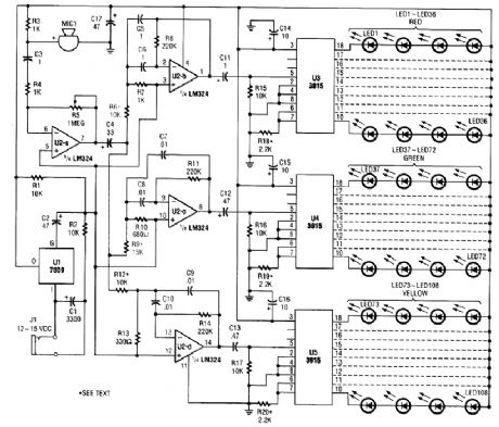
The microphone input, MIC1, is fed through C3 and R4 to inverting amplifier U2-a; the gain of U2-a is controlled by potentiometer R5. The output of U2-a is fed through C4 to the remaining op-arnps (U2-b, U2-c, U2-d), which are all configured as band-pass filters. Each filter is tuned to pass a different range of frequencies by its resistor/capacitor combination. With the values shown, U2-b, U2-c, and U2-d have center frequencies of roughly 100, 1000 and 1500 Hz, respectively.Resistors R6, R9, R12 control the bandwidth and gain of their respective filter circuits, and can range in value from 10 to 15 kΩ. The output of U2-b is capacitively coupled via C11 to the input of U3, with R15 serving as the load resistor for U2-b. That resistor also keeps U3's outputs from float-ing in the absence of a signal. Connected as shown, U3 uses its own internal voltage reference to make a full-scale display of 1.2 V.Each ofthe nlne outputs of U3(output 1 IS not used) sinks four, series-connected (red) LEDs. Op amps U2-c and U2-d qro similarly connected to U4 and U5,respectively, driving green and yellow LED strings,Resistors R18,R19,and R20 control the brightness of their corresponding LED arrays,and they must be adjusted accordingly;different colors of LEDs usually vary in brightness.A lowervalue of resistance will make the LEDs glow brighter.Power for the circuit is supplied by a 500 mA,12-15-Vdc wall-pack transformer,via J1 The out-put ofthe transformer is filtered by 01 arid is regulated by U1;regulation is necessary to keep power-line ripple from affecting the display. The Supply pins of U2 through TTKLJt are bypassed by capacitors014 through C17 to further ensure stability. An on/off switch was deemed unnecessary because thepower Supply should be unplugged when the unit is not in use. (View)
View full Circuit Diagram | Comments | Reading(1020)
PROGRAMMABLE_GAIN_AMPLIFIER
Published:2009/6/18 22:13:00 Author:May

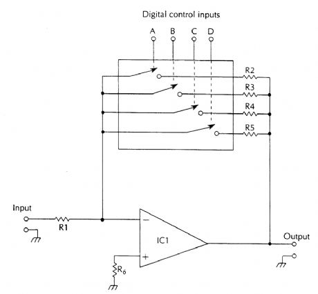
The gain of this amplifier is-Rf/R1 where Rf=effective value of resistance selected by the digital R1 inputs.IC1 op ampIC2 CD4066 quad bilateral switchR1 1-kΩ,1/4-W 5% resistorR2 10-kΩ,1/4-W 5% resistorR3 4.7-kΩ,1/4-W 5% resistorR4 2.2-kΩ,1/4-W 5% resistorR5 1-kΩ,1/4-W 5% resistorR6 2.2-kΩ,1/4-W 5% resistor (View)
View full Circuit Diagram | Comments | Reading(2549)
SLEEP_MODE_CIRCUIT
Published:2009/6/18 22:08:00 Author:May
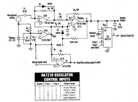
The HA7210 oscillator IC combines with an ICL7642 quad CMOS op amp to produce a sleep-mode control circuit. The circuit is put into the sleep mode with a logic high applied to the Reset input or with an RC timer for automatic reset. The system is awakened by a signal from the microphone/sensor. (View)
View full Circuit Diagram | Comments | Reading(1827)
VOCAL_STRIPPER
Published:2009/6/18 22:06:00 Author:May
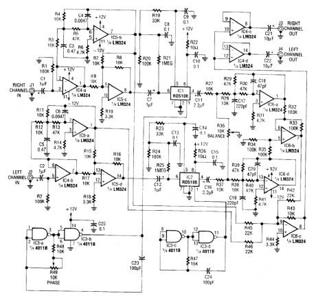


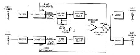
Right- and left-channel signals pass through 1 C4-a and -b buffer amps into active crossover IC5; low frequencies are sent to the ICG-c mixer, and middle and high frequencies are sent to the analog delay lines of 1C1 and 102. That output passes through 1C6-a and -d to filter high-frequency sample steps. IC6-b signals are remixed with low frequencies by ICG-c and are sent to final out via IC4-c and -d buffers.One channel (R) is a variable-delay circuit, using an analog bucket-brigade device and a variable clock frequency. This is compared in amplitude and phase to the L channel (fixed delay). The local can therefore be nulled out via R36. (View)
View full Circuit Diagram | Comments | Reading(1610)
REMOTE_AIVIPLIFIER
Published:2009/6/18 22:02:00 Author:May
Useful for transducers and such where a sin-gle two-wire pair are the only leads available. (View)
View full Circuit Diagram | Comments | Reading(943)
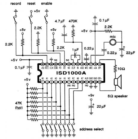
ISD_1000A_RECORD_PLAYBACK_CIRCUIT
Published:2009/6/18 22:00:00 Author:May


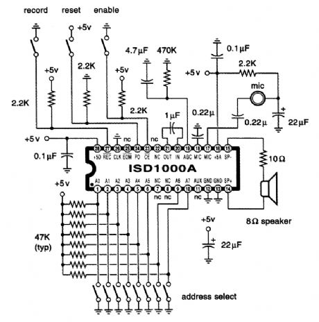
This circuit uses the Information Storage Devices ISD1000A chip(Radio Shack P/N 276-1325). (View)
View full Circuit Diagram | Comments | Reading(2893)
HIGHPASS_AMPLIFIER
Published:2009/6/18 21:55:00 Author:May
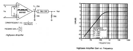
View full Circuit Diagram | Comments | Reading(705)
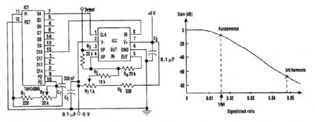
PURE_SINE_WAVE_GENERATOR
Published:2009/6/18 21:55:00 Author:May
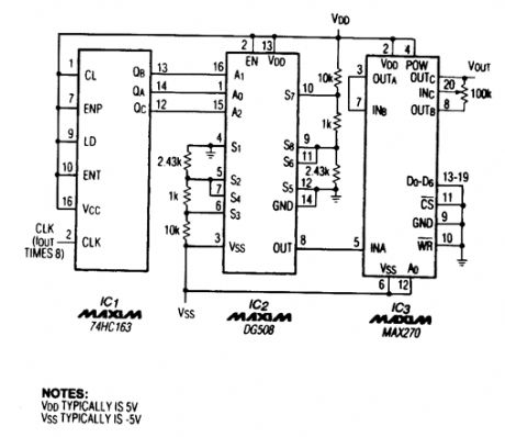
A TTL counter, an 8-channel analog multiplexer, and a fourth-order low-pass filter can generate 10- to 25-kHz sine waves with a THD better than -80 dB. The circuit cascades the two second-order, continuous-time Sallen-Key filters within IC3 to implement the fourth-order low-pass filter.To operate the circuit, choose the filter's cutoff frequency,fC, by tying IC3's D0 through D6 inputs to 5 V or ground. The cutoff frequency can be at 128 possible levels between 1 and 25 kHz, depending on those seven digital input levels. Because the circuit ties D0 through D6 to ground, fC equals 1 kHz. The 100-kΩ potentiometer adjusts the output level between VDD - 1.5 V and VSS + 1.5 V. (View)
View full Circuit Diagram | Comments | Reading(5)
LOWPASS_AMPLIFIER
Published:2009/6/18 21:54:00 Author:May
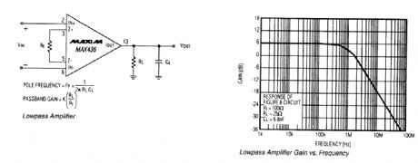
View full Circuit Diagram | Comments | Reading(678)
VCR_HEAD_AMPLIFIER_TESTER
Published:2009/6/18 21:52:00 Author:May
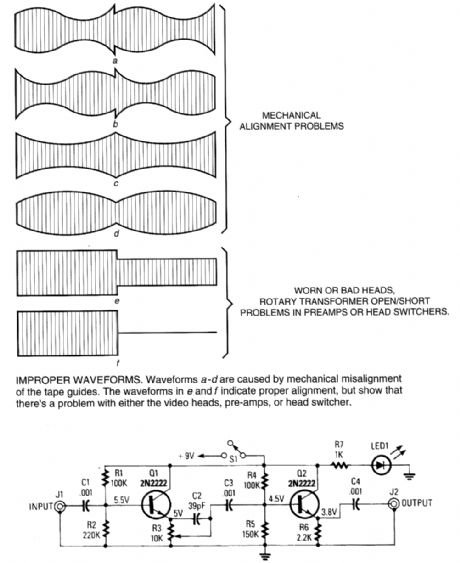
This amplifier enables you to use a signal from a working VCR to test the head amplifiers of a suspected defective VCR.The circuit is basically a video amtplifier. (View)
View full Circuit Diagram | Comments | Reading(741)
SINE_WAVE_SHAPER
Published:2009/6/18 21:51:00 Author:May
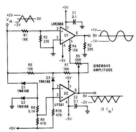
Unlike most sine-wave shapers, this circuit is temperature stable. It varies the gain of a transcon-ductance amplifier to transform an input triangle wave into a good sine-wave approximation. (View)
View full Circuit Diagram | Comments | Reading(3)
SINE_WAVE_GENERATOR
Published:2009/6/18 21:50:00 Author:May
In this circuit, a square wave is filtered by a high-order low-pass filter so that a -3-dB frequency will eliminate most harmonics of the waveform. As a result, the filter outputs a fundamental sine wave. This method is applied to generate a sine wave by using a switched-capacitor filter (MAX292) (see the figure). This circuit offers wide frequency range (0.1 Hz to 25 kHz), low distortion, and con-stant output amplitude throughout the whole frequency range. (View)
View full Circuit Diagram | Comments | Reading(155)
OPERATIONAL_TRANSCONDUCTANCE_AMPLIFIER_WITH_BOOSTER
Published:2009/6/18 21:50:00 Author:May
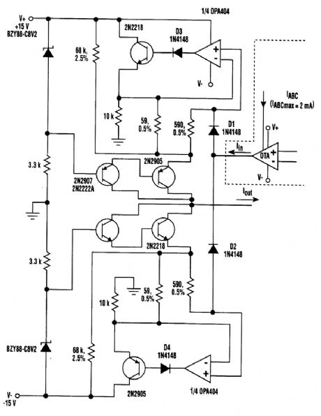
Implementing a bidirectional precision current amplifier in an operational transconductance am-plifier (OTA) can boost the OTA's output current. To accomplish this task, two diodes and a comple-mentary stage are added to this otherwise simple design. (View)
View full Circuit Diagram | Comments | Reading(1100)
| Pages:1416/2234 At 2014011402140314041405140614071408140914101411141214131414141514161417141814191420Under 20 |
Circuit Categories
power supply circuit
Amplifier Circuit
Basic Circuit
LED and Light Circuit
Sensor Circuit
Signal Processing
Electrical Equipment Circuit
Control Circuit
Remote Control Circuit
A/D-D/A Converter Circuit
Audio Circuit
Measuring and Test Circuit
Communication Circuit
Computer-Related Circuit
555 Circuit
Automotive Circuit
Repairing Circuit