
Circuit Diagram
Index 1417
SIMPLE_ANALOG_MULTIPLIER
Published:2009/6/18 21:50:00 Author:May
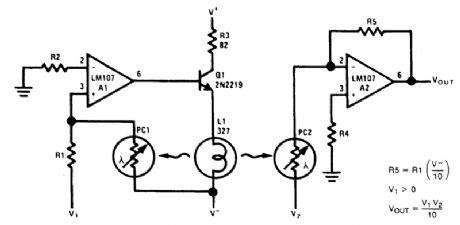
Circuit operation can be understood by considering A2 as a controlled-gain amplifier, amplifying V2, whose gain depends on the ratio of the resistance of PC2 to R5 and by considering A1 as a control amplifier, which establishes the resistance of PC2 as a function of V1. In this way, VOUT, is a function of both V1, and V2.A1, the control amplifier, provides drive for the lamp, L1. When an input voltage, V1, is present, L1 is driven by A1 until the current to the summing junction from the negative supply through POI is equal to the current to the summing junction from V1 through R1. Because the negative supply voltage is fixed, this fordes the resistance of PCl to a value that is proportional to R1 and to the ratio of V1, to V-. L1 also illuminates PC2 and, if the photoconductors are matched, causes PC2 to have a resistance equal to PC1.A2, the controlled gain amplifier, acts as an inverting amplifier whose gain is equal to the ratio of the resistance of PC2 to R5. If R5 is chosen equal to the product of R1, and V-, then VOUT becomes simply the product of V1, and V2. R5 can be scaled in powers of 10 to provide any required output scale factor. (View)
View full Circuit Diagram | Comments | Reading(1798)
SIMPLE_SINE_WAVE_GENERATOR
Published:2009/6/18 21:49:00 Author:May
A 555 timer operating in the astable mode generates the driving pulses and two 4518 dual BCD (binary coded decimal) counters provide the square waves. A TL081 op amp serves as an output buffer-amplifier, and potentiometers R1 and R2 are used in order to control the pulse's frequency and amplitude, respectively.The output-frequency range can be varied by changing CX. For example, a value of 0.1 μF gives a range from about 0.1 to 30 Hz, and avalue of 470 pF gives a range from about 10 Hz to 1.5 kHz. The maxirttum output frequency is 30 kHz. (View)
View full Circuit Diagram | Comments | Reading(2337)
1_Hz_SINE_WAVE_OSCILLATOR
Published:2009/6/18 21:46:00 Author:May
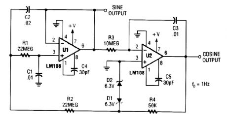
This circuit produces a 1-Hz sine wave using two op amps. A single-chip dual op amp could be used as well. (View)
View full Circuit Diagram | Comments | Reading(1303)
BATTERY_POWERED_SINE_WAVE_GENERATOR
Published:2009/6/18 21:45:00 Author:May
The quality of the sine wave depends on how closely you match the components in the twin-T network in the op amp's feedback loop. (View)
View full Circuit Diagram | Comments | Reading(1168)
WIEN_BRIDGE_SINE_WAVE_OSCILLATOR
Published:2009/6/18 21:43:00 Author:May

This Wien-bridge sine-wave oscillator uses a 2N3819 as an amplitude stabilizer. The 2N3819 acts as a variable-resistance element in the Wien bridge. (View)
View full Circuit Diagram | Comments | Reading(2)
SIMPLE_SINE_WAVE_OSCILLATOR
Published:2009/6/18 21:42:00 Author:May
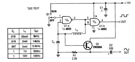
Using an LC circuit,this CMOS oscillator generates slne waves. (View)
View full Circuit Diagram | Comments | Reading(2099)
HIGHLY_STABLE_60_Hz_SINE_WAVE_SOURCE
Published:2009/6/18 21:40:00 Author:May
A highly-stable 60-Hz sine wave can be delivered with this circuit,which offers a different andmuch simpler approach to galnlng a stable amplitude,Capacitor coupling the last stage removes anydc component caused by unequal zener voltages in the clipping circuit that follows the comparator. (View)
View full Circuit Diagram | Comments | Reading(1279)
SHUTDOWN_CIRCUIT
Published:2009/6/18 21:37:00 Author:May
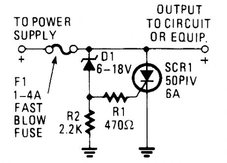
Many modern devices have shutdown circuits that are designed to remove power from the de-vice under power when the voltage rises above a predetermined threshold. This one blows a fuse to protect the device under power. (View)
View full Circuit Diagram | Comments | Reading(929)
RESETTABLE_SHUTDOWN_CIRCUITS
Published:2009/6/18 21:37:00 Author:May
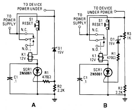
If your circuits experience frequency overvoltage conditions, continually replacing blown fuses can get pretty expensive. However, this shutdown circuit overcomes that deficiency by replacing the fuse with a relay and a low-current SCR. When the input voltage rises above the threshold set by the Zener diode (D1), a current of suf-ficient magnitude is applied to the gate of SCR1, which turns it on. That draws current through the relay coil and energizes it, which swings its commutator to its normally open contact, and disrupts power to the circuit under power. Switch S1, a normally closed pushbutton switch, is used to reset the circuit; it does so by interrupting power to the relay. When S1 is pressed, the relay's wiper arm returns to the normally closed position, restoring power to the connected circuit.If you deal with a number of circuits that have different burn-out levels, try the circuit in B. That circuit variation, a variable trip-point shutdown circuit, allows you to adjust the shutdown threshold to whatever level you desire. The circuit adjustment allows for the 30% variance in the trip point.The zener diode should be selected to have a voltage rating that is slightly lower than the minimum desired threshold voltage. (View)
View full Circuit Diagram | Comments | Reading(950)
SIMPLE_ANALOG_AVERAGING_CIRCUIT
Published:2009/6/18 21:34:00 Author:May

At times,an analog circuit that averages rather than sums call be quite handy. You won’t usually find this type of circuit in op-amp books,possibly because the op amp is used only as a buffer Forbest accuracy,an FET should be used with the offset adjusted out.In addition,the“averagtng”resistors(R1 through R4)should be of Close tolerance.Looldng at the test circuit,op amps 1 through 4 are used to alleviate interaction between adjustment potentiometers P1 through P4 and so that R1 through R4 see the same low impedance.The table shows some arbitrarily set voltages and the resulting output voltage across RL. (View)
View full Circuit Diagram | Comments | Reading(874)
SUBCARRIER_ADAPTER_FOR_FM_TUNERS
Published:2009/6/18 21:32:00 Author:May
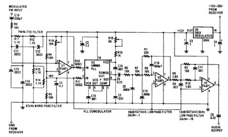
Op amp U1 and its associated components comprise the 67-kHz bandpass filter. A twin-T net-work, comprised offour 1100-Ω resistors and four 0.0022-pF capacitors, is connected in the feed-back network of the op amp. That gives some gain at 67 kHz and heavy attenuation for frequencies above and below that frequency.An additional passive filter at the input to the twin-T network (containing a 220-pF capacitor and a 10,000-Ω resistor) provides some additional roll-off for frequencies below 67 kHz.In practice, the bandpass-filter action covers a frequency range of about 10 kHz above and below the 67-kHz center frequency. Resistor R18 sets the gain of the bandpass-filter stage.Integrated-circuit U2 is a National LM565 phase-locked loop that modulates the 67-kHz fre-quency-modulated (FM) signal from U1. The LM565 PLL consists of a voltage-controlled oscillator (VCO) set to 67 kHz, and a comparator that compares the incoming frequency-modulated 67-kHz signal at pin 2 with the VCO signal that is fed into pin 5.The output of the comparator represents the phase difference between the incoming signal and the VCO signal. Therefore, the output is the audio modulated by the subcarrier. A treble deemphasis of 150 ps is provided by a 0.033-μF capacitor (at pin 7).The free-running VCO frequency is determined by the 0.001-μF capacitor at pin 9 and by the re-sistance between the positive rail and pin 8 (100 Ω in series with R19). Variable-resistor R19 adjusts the oscillator frequency (also known as the centerfrequency) so that the incoming signal is within the lock range of the PLL. (View)
View full Circuit Diagram | Comments | Reading(1116)
SAMPLE_AND_HOLD_CIRCUIT_II
Published:2009/6/18 21:25:00 Author:May
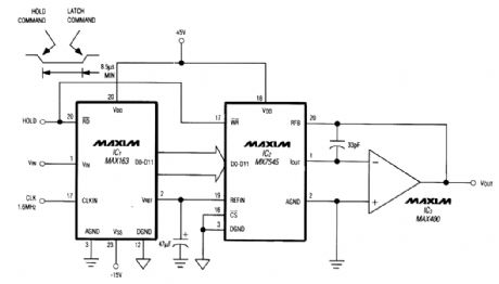
Driving a D/A converter with an A/D converter provides an overall analog-hold function, which though limited in output resolution, offers zero voltage droop and infinite hold time. The A/D converter shown (ICl) includes a 12-bit compatible track/hold at its input. The track/hold specifies a 6-MHz full-power bandwidth, a 30-ns aperture delay, and a 50-ps aperture jitter. The direct connections shown al-low the D/A converter to reconstruct signal levels within the input range of 0 to 5 V. (View)
View full Circuit Diagram | Comments | Reading(0)
SAMPLE_AND_HOLD_CIRCUIT_I
Published:2009/6/18 21:23:00 Author:May
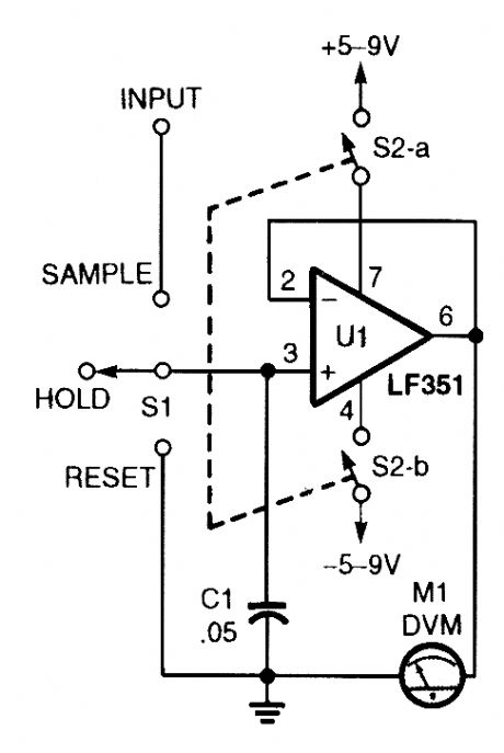
This circuit demonstrates the principle of the sample-and-hold circuit. S1 can be replaced by electronic switches (FET, etc.) in an actual application. (View)
View full Circuit Diagram | Comments | Reading(653)
DIFFERENCE_OF_SQUARES
Published:2009/6/18 21:20:00 Author:May
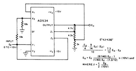
The AD534 is remarkably easy to use in the implementation of the approximation formulas described in Chapter 2-1 of the NonLinectr Circuits Hctndbook. Many of these involve implicit loops to generate the function and previously required several additional op amps for the addition and subtraction of the various terms. This circuit is an example of what can be done with extemal resistors only. For φ between 00 and 900, the approximation maintains a theoretical accuracy to within 0.5% of fullscale; 0.75% is practical with AD534L and 0.1% resistances were used. (View)
View full Circuit Diagram | Comments | Reading(813)
ANALOG_VARIABLE_MULTIPLIER_DIVIDER
Published:2009/6/18 21:09:00 Author:May
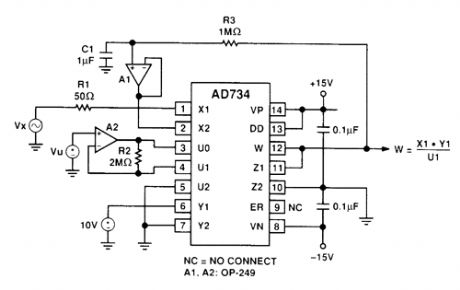
An output voltage (W=X1×Y1/U1) is produced by Lhis multiplier circuit The AD734 is a fourquadrant multiplier. (View)
View full Circuit Diagram | Comments | Reading(1002)
SQUARE_ROOTER
Published:2009/6/18 21:03:00 Author:May
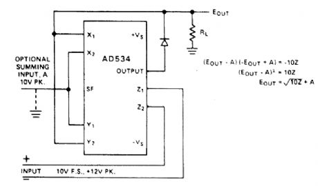
This illustration shows the connection of the AD534 for square-rooting, with differential inputs.The diode prevents a latching condition-common to this conftguration-which would occur if the input momentarily changed polarity. As shown, the output is always positive; it can be changed to a negative output by reversing the diode polarity and interchanging the X inputs. Because the signal input is differential, all combinations of input and output polarities can be realized. If the output circuit does not provide a resistive load to ground, one should be connected to maintain diode conduc-tion. For critical applications, the Z offset can be adjusted for greater accuracy below1 V. (View)
View full Circuit Diagram | Comments | Reading(882)
BRIDGE_LINEARIZING_FUNCTION
Published:2009/6/18 20:57:00 Author:May
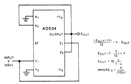
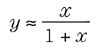
If one arm of a Wheatstone Bridge varies from its nominal value by a factor,(1 + 2x), the voltage or current output of the bridge will be(with appropriate polarities):Linear response requires very small x and,usually,prearrtplification.The circuit shown here enables Iarge-deviation bridges to be used without losing linearity.The circuit computes the inverse of the bridge function, i.e.,Depending on which arm of the bridge varies, it might be necessary to reverse the polarity of the z connections. (View)
View full Circuit Diagram | Comments | Reading(778)
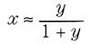
QRP_TRANSCEIVER_FOR_18,21,AND_24_MHz
Published:2009/6/18 5:40:00 Author:May
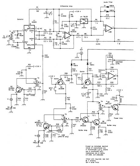
This CW transceiver has 1.25 to 4 W RF output, a direct-conversion receiver, full break-in, and SW sidetone generation.The power supply is 13.8 V, which makes this transceiver suitable for mobile or portable operation. (View)
View full Circuit Diagram | Comments | Reading(3499)
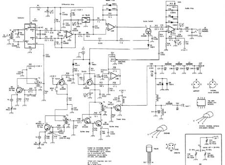
49_MHz_FM_TRANSMITTER
Published:2009/6/18 5:22:00 Author:May
This 49-MHz FM transmitter consists of an audio amplifier, a low-pass filter, three RF stages, and a regulated-dc power supply. The output is about 16 mW into a 50-Ω load. This transmitter can be used in many 49-MHz applications, such as in a baby monitor, cordless telephone, or in conjunction with a scanner as a one-way voice link. (View)
View full Circuit Diagram | Comments | Reading(3208)
TRACKING_TRANSMITTER
Published:2009/6/18 5:15:00 Author:May
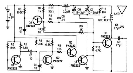
This tracking transmitter consists of four distinct subassemblies; a free-running multivibrator, a transmit switch, an audio-tone generator, and an FM transmitter. The multivibrator (which produces a pulse width with a pulse separation of 1500 ms) is built around Q1 and Q2. The multivibrator out-put is coupled through R5 to the base of Q3, whose emitter feeds Q4, which controls the circuit's transmitter section. (View)
View full Circuit Diagram | Comments | Reading(286)
| Pages:1417/2234 At 2014011402140314041405140614071408140914101411141214131414141514161417141814191420Under 20 |
Circuit Categories
power supply circuit
Amplifier Circuit
Basic Circuit
LED and Light Circuit
Sensor Circuit
Signal Processing
Electrical Equipment Circuit
Control Circuit
Remote Control Circuit
A/D-D/A Converter Circuit
Audio Circuit
Measuring and Test Circuit
Communication Circuit
Computer-Related Circuit
555 Circuit
Automotive Circuit
Repairing Circuit