
Circuit Diagram
Index 1420
TOUCH_SWITCH_II
Published:2009/6/18 4:10:00 Author:May
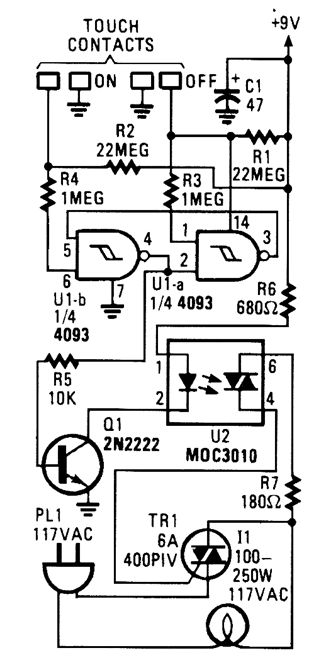


When the touch-on contacts are bridged, pin 6 of U1-b goes low, which forces its output (the set output) at pin 4 to go high. That high divides along two paths: in one path, the output is applied to pin 2 of UI-a, which causes its out-put at pin 3 to go low. That low is, in turn, ap-plied to pin 5 of UI-b, which latches the gate in a high output state. In the other path, the out-put of U1-b is used to drive Q1. When Q1 turns on, U2's internal LED lights, which turns on its internal, light-sensitive, triac-driver (diac) out-put element. The triac driver feeds gate current to TRI, causing it to turn on, and light the lamp (11).When the off contact is bridged, UI-a's out-put switches and latches high, causing UI-b's output to go low, turning off the lamp. (View)
View full Circuit Diagram | Comments | Reading(377)
BASIC_OP_AMP_DIFFERENTIAL_AMPLIFIER
Published:2009/6/18 4:07:00 Author:May

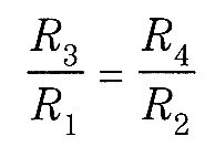
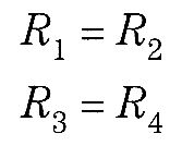

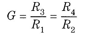
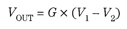


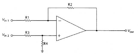


In most cases, R1 is equal to R2 and R3, has the same value as R4 These equalities don't always have to be true, but they do significantly simplify the circuit design in most practical applications. In any case, for a true differential amplifier, the R3,:R1and R2;R4 ratios must be equal. That is:The circuit still functions even if these ratios are not maintained, but the signals at the inverting and noninverting inputs are subjected to differing amounts of gain, which would be undesirable in most practical applications.These resistance ratioi determine the gain of the amplifier:Assuming that the resistance ratios are maintained, the output voltage is equal to the differences between the two input voltages, multiplied by the gain. That is, (View)
View full Circuit Diagram | Comments | Reading(1013)
TOUCH_SWITCH_I
Published:2009/6/18 4:04:00 Author:May
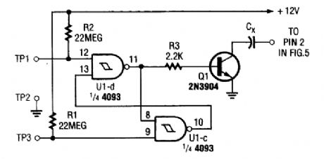
Two NAND Schmitt triggers are connected in a flip-flop configuration to produce a bridged touch-activated switch. (View)
View full Circuit Diagram | Comments | Reading(1128)
ac_NOISE_DETECTOR
Published:2009/6/18 4:04:00 Author:May
This circuit can be added to the glitch detector to trigger on ac noise. (View)
View full Circuit Diagram | Comments | Reading(903)
455_kHz_AM_DETECTOR
Published:2009/6/18 4:03:00 Author:May
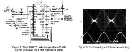
The LTC1278 undersamples the 455-kHz carrier to recover the 5-kHz modulating signal. The ap-plication shown uses the LTC1278 to undersample (at 227.5 ksps) a 455-kHz IF amplitude-modu-lated by a 5-kHz sine wave. Figures 26-19A and 26-19B show, respectively, the 455-kHz IF carrier and the recovered 5-kHz sine wave that results from a 12-bit DAC reconstruction. (View)
View full Circuit Diagram | Comments | Reading(902)
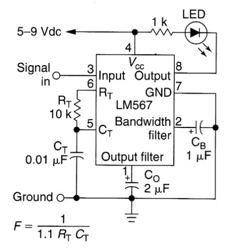
BRIDGING_TOUCH_PLATE_SENSOR__
Published:2009/6/18 4:03:00 Author:May

In this circuit, two 567 tone decoders are used. One is an oscillator, the other is a detector.Bridging TP1 and TP2 causes U2 to receive UI's signal, which causes pin 8 of U2 to go low. This ac-tion lights LED1 and drives the output of Q2 high. (View)
View full Circuit Diagram | Comments | Reading(1686)
LOW_COST_ONE_QUADRANT_MULTIPIER_DIVIDER
Published:2009/6/18 4:02:00 Author:May

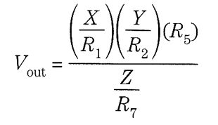
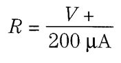
This circuit will produce an output that is proportional to the product of the (JQ and ()] inputs divided by the Z input. All inputs must be positive, limiting operation to one quadrant.For very low level inputs, the offset voltage in the LM308s might create large percentage errors referred to input. A simple scheme for offsetting any of the LM308s to zero is shown in dotted line; the positive input of the appropriate LM308 is simply tied toRX instead of ground for zeroing. The summing mode of operation on all inputs allows easy scaling on any or all inputs. Simply set the input resistor equal to (Vin(max)/200μA). Vout is equal to:Input voltages above the supply voltage are allowed because of the sumrning mode of operation. Several inputs can be summed at X,Y,and Z.For a simple {X)·(Y) or (X)/Z function, the unused input must be tied to the reference voltage. Perturbations in this reference will be seen at the output as scale factor changes, so a stable refer-ence is necessary for precision work. For less critical applications, the unused input can be tied to the positive supply, with (View)
View full Circuit Diagram | Comments | Reading(885)
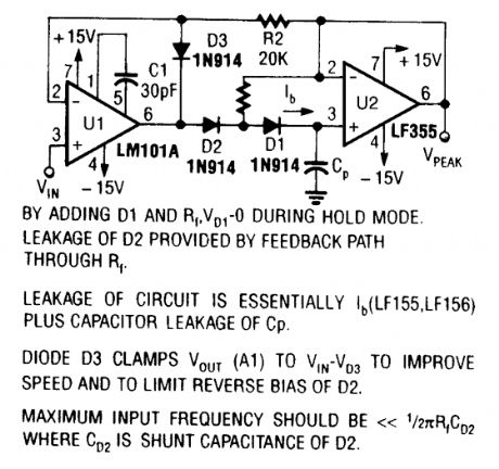
POSITIVE_PEAK_DETECTOR
Published:2009/6/18 4:01:00 Author:May
View full Circuit Diagram | Comments | Reading(0)
NEGATIVE_PEAK_DETECTOR
Published:2009/6/18 4:01:00 Author:May
View full Circuit Diagram | Comments | Reading(0)
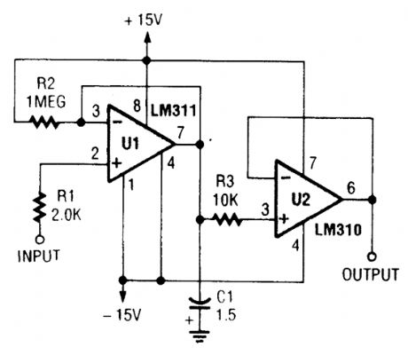
LOW_DRIFT_PEAK_DETECTOR
Published:2009/6/18 4:00:00 Author:May
View full Circuit Diagram | Comments | Reading(0)
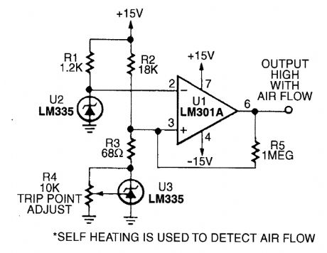
AIR_FLOW_DETECTOR
Published:2009/6/18 3:59:00 Author:May
View full Circuit Diagram | Comments | Reading(0)
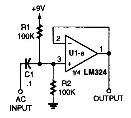
BASS_TONE_CONTROL
Published:2009/6/18 3:58:00 Author:May
The frequency dependence of the capacitor's impedance permits this circuit to boost the bass frequencies. (View)
View full Circuit Diagram | Comments | Reading(1337)
SWITCH_CLOSURE_CIRCUIT
Published:2009/6/18 3:58:00 Author:May
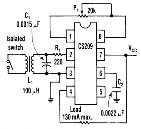
A standard proximity detector circuit for the Cherry Semiconductor CS209 IC can detect an iso-lated switch closure by adding a few tums of wire around the circuit's inductor (Radio Shack 273-102). Moreover, the technique doesn't require any isolated power (see the figure). With the switch open, the potentiometer P1 is adjusted until the output switches off. When the switch is closed, the Q of the circuit changes and the output turns on. Capacitor C1 should be silvered mica, and poten-tiometer P1 should be a multiturn type such as the Boums 3006P-1-203. A 9-V supply can be used for Vcc. (View)
View full Circuit Diagram | Comments | Reading(1137)
TREBLE_TONE_CONTROL
Published:2009/6/18 3:58:00 Author:May

The treble control has capacitors placed in series with the potentiometer. (View)
View full Circuit Diagram | Comments | Reading(733)
COMBINED_BASS_AND_TREBLE_CONTROLS
Published:2009/6/18 3:57:00 Author:May
Bass and treble circuits can be combined to form a two-control here. (View)
View full Circuit Diagram | Comments | Reading(887)
CRTSTAL_RADIO_DETECTOR
Published:2009/6/18 3:57:00 Author:May
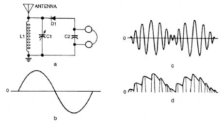
This is a crystal detector receiver with headphones (Fig. 26-13A), audio-frequency signal (Fig.26-13B), modulated signal (Fig. 26-13C), and a demodulated wave (Fig. 26-13D). (View)
View full Circuit Diagram | Comments | Reading(878)
15_kHz_TONE_DETECTORLED
Published:2009/6/18 3:55:00 Author:May
This circuit detects the presence of a 15-kHz audio signal and light the LED when it does so. (View)
View full Circuit Diagram | Comments | Reading(735)
SINGLE_COMPARATOR_WINDOW_DETECTOR
Published:2009/6/18 3:54:00 Author:May
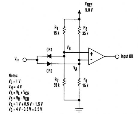
Simply by adding two steering diodes, a window detector can be built using only a single com-parator. The detector performs well for windows of about 1 V or greater, but it isn't suitable where extreme precision is required because the forward drops of the diodes vary.In the basic circuit, two resistive dividers set threshold voltage levels at both the inverting and noninverting inputs of the comparator by dividing the reference voltage. The input voltage is steered to the appropriate comparator input by diodes CR1 and CR2.When the input voltage is within the window, neither diode conducts, and the comparator is bi-ased for a high output. When the input goes above the window, CR2 conducts and pulls the inverting input high, causing the comparator output to go low. When the input voltage goes below the window, CR1 conducts, pulling the noninverting input low, again causing the comparator output to go low. The source resistance of Vinmust be low compared to the equivalent parallel resistance of each divider. (View)
View full Circuit Diagram | Comments | Reading(1620)
HAM_BAND_VFO
Published:2009/6/18 3:54:00 Author:May
This basic VFO for the 3- to 6-MHz range is commonly used in amateur applications, using a Col-pitts circuit. For 5 to 5.5 MHz, C1 = C2 = 70 pF and for 3.5 to 4.0 MHz, use 1000 pF. C3 is typically 10 to 220 pF, depending on the frequency. C4, C5, and C6, together with C3, determine the frequency along with L1. C6 can be made up of several smaller values, paralleled to get the exact required value. (View)
View full Circuit Diagram | Comments | Reading(1022)
REPEATER_TONE_BURST_GENERATOR
Published:2009/6/18 3:52:00 Author:May
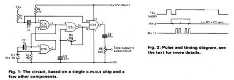
Integrated circuit gates IC1-a and ICl-b form a monostable, whose time constant is determined by C2 and R3. When the transmitter is dekeyed (and then almost immediately rekeyed) point TX+ goes low and takes pin 1 low for a short time. This triggers the start of the timing period controlled by C2/R3, The capacitor C2, charges via R3 until the trigger point of gate ICl-b is reached. At this point, the monostable changes state and pin 3 goes low again. On the prototype, this time was about 700 ms. The pulse occurs each time after dekeying and it is normally inaudible. If, however, point TX+ goes high again (as in immediate rekeying) the monostable is still in the enabled state and the oscillations of ICl-c are present in the transmission. During this time period, the buffer gate, ICl-d, is enabled and the tone is therefore passed to the output. (View)
View full Circuit Diagram | Comments | Reading(1003)
| Pages:1420/2234 At 2014011402140314041405140614071408140914101411141214131414141514161417141814191420Under 20 |
Circuit Categories
power supply circuit
Amplifier Circuit
Basic Circuit
LED and Light Circuit
Sensor Circuit
Signal Processing
Electrical Equipment Circuit
Control Circuit
Remote Control Circuit
A/D-D/A Converter Circuit
Audio Circuit
Measuring and Test Circuit
Communication Circuit
Computer-Related Circuit
555 Circuit
Automotive Circuit
Repairing Circuit