
Circuit Diagram
Index 1421
A_SHORTWAVE_PULSED_MARKER_OSCILLATOR
Published:2009/6/18 3:52:00 Author:May
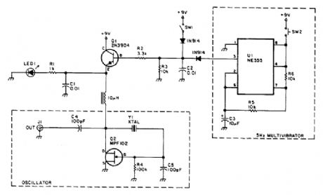
A useful marker oscillator can be made using an NE555 to pulse the oscillator at an audio rate. This makes it easy to find the signal in the presence of interference. The crystal can be any suitable frequency from 1 to 30 MHz. (View)
View full Circuit Diagram | Comments | Reading(817)
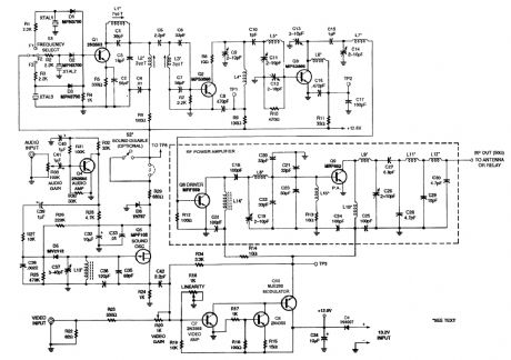
MINI_ATV_TRANSMITTER
Published:2009/6/18 3:52:00 Author:May
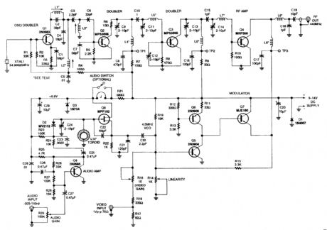
This low-power NTSC video and sound transmitter is useful for amateur radio, video handle-talkie, R/C and surveillance pur-poses. A crystal oscillator-multip lier RI' power amplifier. Video modulation is via a three-transistor series modulator. The sound subcarrier is generated with a VC0 circuit and is combined with the video information. The output is 0.4 to 1.2 W with supply volt-ages of 9 to 14 volts. A complete kit of parts, including PC board, is available from North Country Radio, P.O. Box 53, Wykagyl Sta-tion, New Rochelle, NY 10804-0053A. (View)
View full Circuit Diagram | Comments | Reading(2883)
LM556_FREQUENCY_DETECTOR
Published:2009/6/18 3:51:00 Author:May
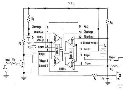
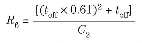
The circuit (see the ftgure), is built around an LM556 dual-timer IC. The 556's first timer is wired as a one-shot and is used to stretch the incoming pulses into fixed-length pulses. The second timer, which is similar to an astable multivibrator (pin 13 remains disconnected), functions as follows:The one-shot's fixed-length pulses, which are output on pin 5, turn on Q1 and discharge C2 through R5. If the frequency of the pulses is high enough, the voltage on C2 will fall below1/3 VCC and the second timer's output, pin 9, will go to a logic 1. Conversely, if the frequency is low enough or is zero, the voltage on C2 will charge through R6 to a level above2/3 VCC, and the pin 9 output will go to a logic 0. The idea is to keep the upper and lower peak voltage on C2 below 2/3 VCC and1/3 VCC, respectively for a logic 1, and above2/3 VCC and1/3 VCC, respectively, for a logic 0.To find the one-shot values, R3 and C1, select a pulse width (1.1 × R3 × C1) that's greater than the largest input pulse width and less than twice the inverse of the highest input frequency. To find R5, R6, and C2, first determine the duty cycle (ton/toff) of the input signal. Next, choose a standard value for C2 and calculate R6:Also, R5 = R6 (ton/toff). A tweak of resistors R5 and R6 might be needed to get the preferred response. Input signals with low duty cycles work the best. Finally, notice that capacitors C3 and C4 can be any value between 0.01 and 0.1 μF. (View)
View full Circuit Diagram | Comments | Reading(3040)
NE6O2_RF_OSCILLATOR_CIRCUITS
Published:2009/6/18 3:50:00 Author:May
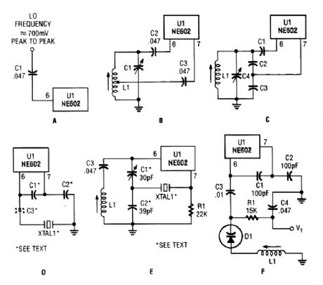
Just about any standard oscillator (such as a Colpitts or Hartley configuration) can be used to generate the LO (local oscillator) frequency needed by the NE602. (View)
View full Circuit Diagram | Comments | Reading(942)
TWO_TONE_ENCODER
Published:2009/6/18 3:49:00 Author:May
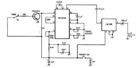
Using an XR2206 oscillator, this circuit can generate two audio tones. Switching between tones can be done with a logic level to either the base of the PN2222 or pin 9 of the XR2206. (View)
View full Circuit Diagram | Comments | Reading(0)
5_W_ATV_TRANSCEIVER
Published:2009/6/18 3:48:00 Author:May
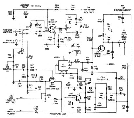
For the transmitter schematic (part of this transceiver), see entry entitled S-W ATV Transmit-ter for 440 MHz, Fig. 5-1. The downconverter portion is shown here.This transmitter contains both a video and sound section. Five to six watts PEP on synch tips of NTSC video are produced. Three channels are available. Channel switching is via PIN diodes. Power supply voltage is 12 to 14 Vdc. The receiver function is provided with a downconverter circuit and is tunable. A relay is used for T-R switching. A complete kit of parts, including PC board, is available from North Country Radio, P.O.Box 53, Wykagyl Station, New Rochelle, NY 10804-0053A. (View)
View full Circuit Diagram | Comments | Reading(2137)
EXTENDED_ON_TIME_TIMER
Published:2009/6/18 3:45:00 Author:May


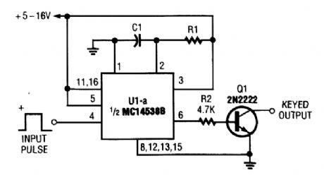

Half of a Motorola MC14538B dual, precision, retriggerable monostable multivibrator is used to form an extended on-time timer circuit. That type of circuit can be used as a switch debouncer. Such circuits are often used in digital circuitry, where each and every bounce of a switch contact is seen as a separate digital input.The delay on tirne (established by C1 and R1) is easily set using the formula, C1xR1, =T, where C1 is in microfarads,R1, is in megohms, and T is in seconds. (View)
View full Circuit Diagram | Comments | Reading(2970)
5_W_ATV_TRANSMITTER_FOR_440_MHz
Published:2009/6/18 3:45:00 Author:May
The circuit will produce typically 6 W RE output on synch tips. A crystal oscillator drives a doubler to produce a 220-MHz output.Another doubler produces 440 MHz to drive the power amplifier. A high-level series modulator provides the video modulation capa-bility. A sound subcarrier is generated using a VCO circuit and combined with the video information. A complete kit of parts, includ-ing the PC board, is available from North Country Radio, P.O.Box 53, Wykagyl Station, New Rochelle, NY 10804-0053A. (View)
View full Circuit Diagram | Comments | Reading(1759)
POPULAR_ELECTRONICS
Published:2009/6/18 3:42:00 Author:May
View full Circuit Diagram | Comments | Reading(1106)
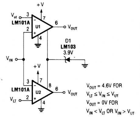
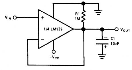
DOUBLE_ENDED_LIMIT_DETECTOR
Published:2009/6/18 3:42:00 Author:May
View full Circuit Diagram | Comments | Reading(0)
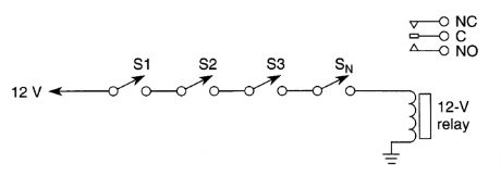
RELAY“OR”CIRCUIT
Published:2009/6/18 3:41:00 Author:May
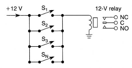
Closing any switch S1,S2,S3,or Sn will actuate the relay(N=any number).Use this circuit for burglar alarms,etc. (View)
View full Circuit Diagram | Comments | Reading(630)
NEGATIVE_PEAK_DETECTOR
Published:2009/6/18 3:41:00 Author:May
View full Circuit Diagram | Comments | Reading(0)
GRID_LEAK_DETECTOR
Published:2009/6/18 3:41:00 Author:May
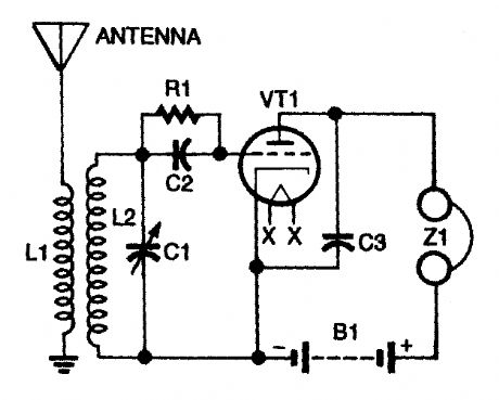
Tuned-cirfuit receiver with grid-leak detection. (View)
View full Circuit Diagram | Comments | Reading(982)
COUNT_DOWN_TIMER
Published:2009/6/18 3:41:00 Author:May
With switch S1 in the off position, as shown, battery voltage is applied across timing-capacitor C1, which stays chargedwhile the rest of the circuitryhas no power supplied to it. Transistor Q1, and thus transistors Q2 through Q4, are kept in an off condition as long as C1 has a sufficient charge. (View)
View full Circuit Diagram | Comments | Reading(805)
RELAY“AND”CIRCUIT
Published:2009/6/18 3:37:00 Author:May
All switches 51 through Sn must be closed to operate the relay.If one opens,the relay drops out.Use this circuit for burglar alarms,etc. (View)
View full Circuit Diagram | Comments | Reading(639)
LONG_DELAY_PERIOD_TIMER
Published:2009/6/18 3:37:00 Author:May
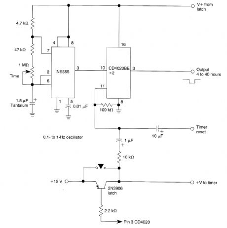
This method of obtaining a 4 to 40 hour timing period from a 555 IC can be further expanded to produce even longer delays with equal accuracy. (View)
View full Circuit Diagram | Comments | Reading(1284)
VCR_VIDEO_DETECTOR_CONTROLLER
Published:2009/6/18 3:36:00 Author:May
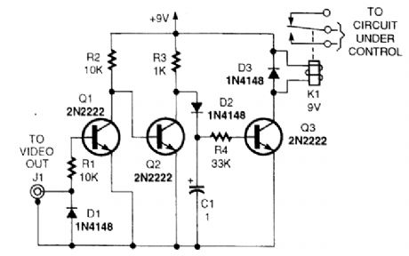
This circuit uses the video output from a VCR or camera to control a relay. Video turns on Q1, cutting off Q2, allowing Q3 to be forward biased, activating relay K1. You can use the timer in your VCR and this unit to generate long time delays as well. (View)
View full Circuit Diagram | Comments | Reading(1499)
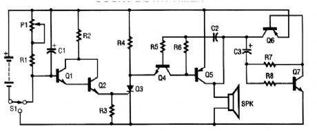
MOBILE_RADIO_ON_ALARM_TIMER
Published:2009/6/18 3:33:00 Author:May

This system will prevent you from accidentally leaving your mobile radio on, draining the battery.LED1 will light when the vehicle's ignition is on, or while the car is running. Switch S1 in the ON po-sition will close relay K1, completing the power circuit to the equipment. If the ignition switch is shut off, and switch S1 is still in the ON position, an alarm (piezo) will begin to beep and LED2 will flash.Returning S1 to the center position will shut everything off. If equipment operation is desired after shutting off the vehicle, you can place switch S1 in the AUT0 position and momentarily press S2, a normally open push-button switch. Depressing this switch begins a timing cycle. The length of time that the Mobile-ON alarm/timer operates before shutting everything off can be prograrrtmed by se-lecting R6. The approximate time delays are provided in the chart with the schematic. Or, you could change the value of C6. These components control the holding time of relay K1. LED3 will light while the circuit is in AUT0 status. Incidentally, you can also cartcel the time delay at any time during the delay period by simply switching it off. (View)
View full Circuit Diagram | Comments | Reading(720)
GLITCH_DETECTOR
Published:2009/6/18 3:33:00 Author:May
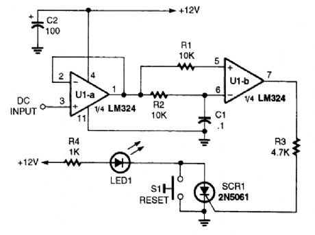
In the circuit, two op amps (half of an LM324 quad op amp) and an SCR are direct coupled in a dc-voltage monitoring circuit. Op-amp UI-a is configured as a voltage follower, which feeds the bridged in-puts of the second op amp, U1-b. A resistor/capacitor combination (R2/C1) connected to the negative input of U1-b forms an RC time-delay circuit. As long as there is no change in the dc-voltage level at either of UI-b's inputs, its output is near zero. If a voltage glitch occurs, the RC timing circuit will delay the voltage change at the op amp's inverting input, causing its output to go high, triggering SCR1 and causing LED1 to light. The circuit's sensitivity allows it to detect voltage changes in the millivolt range.Pressing S1 diverts the SCR's holding current to ground, causing it to turn off and reset the circuit. (View)
View full Circuit Diagram | Comments | Reading(2116)
WIDE_RANGE_TIMER_lMINUTE_TO_400_HRS
Published:2009/6/18 3:33:00 Author:May
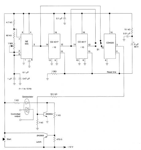
This ultra wide range timer uses a 555 timer base, two 4017Bs and a 4020B that act as frequency dividers that can be switched in and out. S1 is a SP3T range switch. (View)
View full Circuit Diagram | Comments | Reading(995)
| Pages:1421/2234 At 2014211422142314241425142614271428142914301431143214331434143514361437143814391440Under 20 |
Circuit Categories
power supply circuit
Amplifier Circuit
Basic Circuit
LED and Light Circuit
Sensor Circuit
Signal Processing
Electrical Equipment Circuit
Control Circuit
Remote Control Circuit
A/D-D/A Converter Circuit
Audio Circuit
Measuring and Test Circuit
Communication Circuit
Computer-Related Circuit
555 Circuit
Automotive Circuit
Repairing Circuit