
Circuit Diagram
Index 1437
FREQUENCY_MULTIPLIER_WITHOUT_PLL
Published:2009/6/17 1:53:00 Author:May
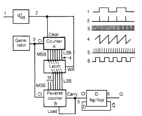
An input rectangular signal is differentiated and short impulses are formed from its edges. These impulses write the content of counter A to a latch that clears the counter after a very short time. Counter A counts impulses of the frequency fo that are much greater than that of the input signal. The pulses come from an impulse generator. Thus, the number, which is written to the latch, expresses the number of these intpulses between the edges of the input signal. The impulses from the same generator pass to (reverse) counter B. The carry impulse loads the content of the latch to counter B. The latch is connected with the reverse counter such that the number written to this counter is 2M times smaller than the number introduced to the latch. This can be readily achieved by omitting M most significant bites of counter B. Because the number loaded to counter B is 2M times smaller than the number in the latch, the carry impulses of counter B have frequency 2M times greater than the frequendy of the impulses at the output of the differentiator. The cany impulses are fed to a D flip-flop, which divides their frequency by two. In this way, the output frequency is 2M greater than input frequency fo as long as the frequency of impulse generator fg is much greater than 2Mfo. (View)
View full Circuit Diagram | Comments | Reading(1006)
RELAY_FUSE_FOR_BATTERY_CHARGES
Published:2009/6/17 1:53:00 Author:May
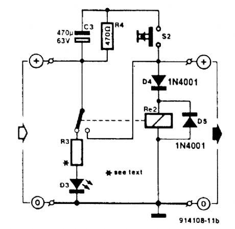
Charged capacitor C3 and momentary push-button switch S2 are used to momentarily energize relay RE2. The batte:y under charge energizes the relay to hold it closed. S2 will energize the relay even if the battery is too far discharged initially to energize it. (View)
View full Circuit Diagram | Comments | Reading(928)
LIGHT_SEQUENCER
Published:2009/6/17 1:52:00 Author:May


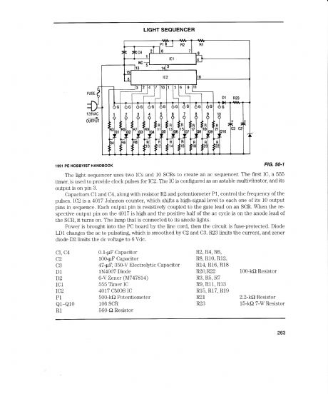
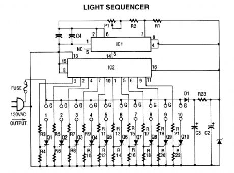
The light sequencer uses two ICs and 10 SCRs to create an ac sequencer. The first IC, a 555 timer, is used to provide clock pulses for IC2. The IC is configured as an astable multivibrator, and its output is on pin 3.Capacitors C1 and C4, along with resistor R2 and potentiometer PI, control the frequency of the pulses. IC2 is a 4017 Johnson counter, which shifts a high-signal level to each one of its 10 output pins in sequence. Each output pin is resistively coupled to the gate lead on an SCR. When the re-spective output pin on the 4017 is high and the positive half of the ac cycle is on
the anode lead of the SCR, it turns on. The lamp that is connected to its anode lights.Power is brought into the PC board by the line cord, then the circuit is fuse-protected. Diode LD1 changes the ac to pulsating, which is smoothed by CZ and C3. R23 limits the current, and zener diode D2 limits the dc voltage to 6 Vdc.
CI,040.1-μF Capacitor R2,R4,R6,C2 100-μF Capacitor R8,R10,R12,C3 47-μF, 350-V Electrolytic Capacitor R14,R16,R18D1 1N4007 Diode R20,R22 100-kΩ ResistorD2 6-V Zener (M747814)R3,R5,R7IC1 555 Timer IC R9,R11,R13IC24017 CMOS IC R15,R17,R19P1 500-kΩ Potentiometer R21 2.2-kΩ ResitstorQ1-Q10 106 SCR R23 15-kΩ 7-W ResistoR1 560-Ω Resistor (View)
View full Circuit Diagram | Comments | Reading(3196)
CAR_BATTERY_AND_ALTERNATOR_MONITOR
Published:2009/6/17 1:51:00 Author:May
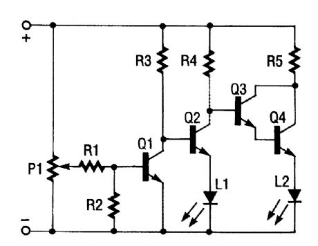
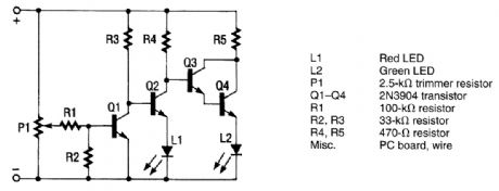
The monitor is a simple voltage comparator in which a car battery serves as the battery for op-eration. The input voltage to the comparator is set by adjustment potentiometer P1, which must be adjusted so that the green LED L2 is on when the altemator is operating properly and red LED1 is on when the altemator is inoperative.The circuit operates as follows: When the alternator operates properly, the battery voltage is higher and P1 is set so that transistor Q1 causes Q2 to be off. That results in Q3 and Q4 being fully on, thus applying current to green LED L2. If the battery voltage is lowered (alternator inoperative), transistor Q1 is turned off. That allows transistor Q2 to turn fully on, applying current to red LED L1, indicating trouble. Once Q2 is on, it causes Q3 and Q4 to go out of conduction. (View)
View full Circuit Diagram | Comments | Reading(1538)
0_2_A_BATTERY_CURRENT_MONITOR_WITH_DIGITAL_OUTPUT
Published:2009/6/17 1:49:00 Author:May
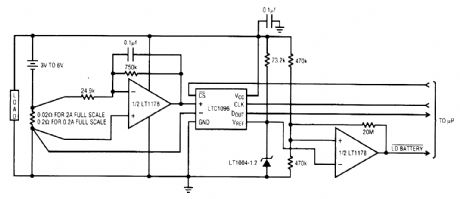
IC devices by Linear Technology make up this current monitor circuit 3- to 6-V battery. (View)
View full Circuit Diagram | Comments | Reading(733)
BATTERY_SAVER_CIRCUIT
Published:2009/6/17 1:48:00 Author:May
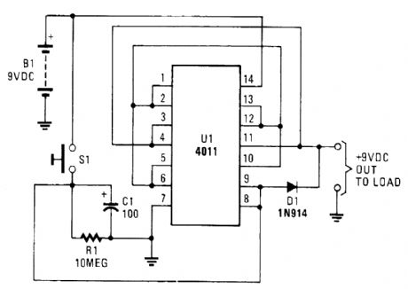
This battery saver circuit can automatically turn off a small piece of test equipment after a desired period of time, allowing you to leave your shop worry free.This circuit uses a CD4011 IC to act as a simple timer. One section acts as an RC discharge timer (pin 7). This causes its output to go low, holding the three other outputs high acting as a 9-V source.After C1/R1 discharges approximately 10 minutes, the output drops to zero. S1 resets the circuit. (View)
View full Circuit Diagram | Comments | Reading(3229)
BATTERY_VOLTAGE_MONITOR
Published:2009/6/17 1:45:00 Author:May
When battery voltage goes low, pin 4 of U1 goes high as Q1 fails to conduct. This activates oscillator U1 and generates audio tone. R5 sets level at which the circuit activates. (View)
View full Circuit Diagram | Comments | Reading(1012)
BATTERY_TEST_CIRCUIT
Published:2009/6/17 1:44:00 Author:May
Using this circuit, three levels of voltage can be displayed-normal (11 to 15 V), high (>15 V), and low (<11 V). When the voltage is low, the LED glows steadily. In the normal range, the LED is off. When the voltage is high, the LED blinks at a 1-Hz rate. This circuit is useful for assuring proper electrical system operation. (View)
View full Circuit Diagram | Comments | Reading(749)
BATTERY_WATCHDOG
Published:2009/6/17 1:42:00 Author:May
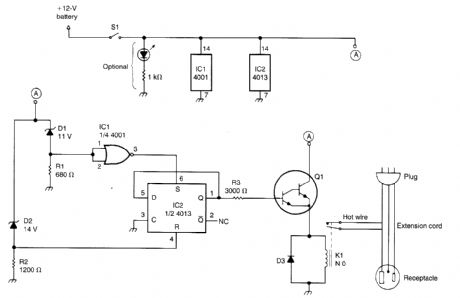
This circuit uses a pair of Zener diodes to monitor battery voltage of a 12-V battery. If below 11 V, D1 ceases to conduct, pin 3 of IC2 goes high, setting FF IC2 turning on Q1, K1, and the battery charger. At excess of 14-V battery voltage (full charge), D2 conducts, resetting FF IC2, and cutting off the battery charger. (View)
View full Circuit Diagram | Comments | Reading(797)
VISIBLE_LIGHT_AUDIO_TRANSMITTER
Published:2009/6/17 1:42:00 Author:May
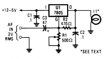
In the visible-light transmitter, a 7805 volt-age regulator is connected in a variable-voltage configuration, and an audio signal is fed to the common input, to modulate the output voltage.The modulated output voltage is used to transmit intelligence via an incandescent larnp.
(View)
View full Circuit Diagram | Comments | Reading(1272)
VISIBLE_LIGHT_RECEIVER
Published:2009/6/17 1:41:00 Author:May
This receiver for amplitude-modulated light signals uses phototransistor Q1 mounted in a para-bolic reflector (to increase range). Any npn phototransistor should work. Emitter-follower Q2 drives amplifier Q3. The output from Q3 feeds volume control R7 and audio amplifier UI. A 9- to 12-V supply is recommended for the receiver. (View)
View full Circuit Diagram | Comments | Reading(1081)
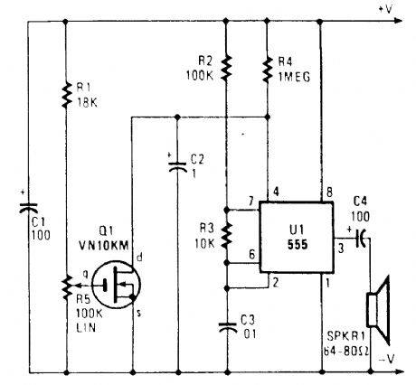
SUPPLY_VOLTAGE_MINITOR
Published:2009/6/17 1:38:00 Author:May
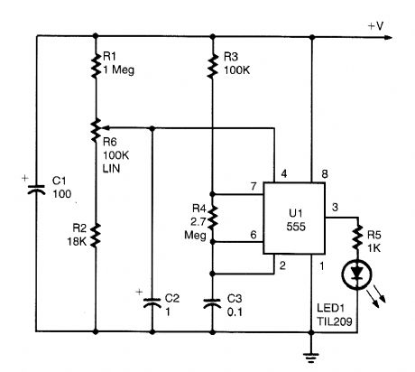
When supply voltage exceeds a preset level, the 555 oscillates, and flashes LED1. The flash rate is controlled by varying C3. (View)
View full Circuit Diagram | Comments | Reading(959)
LED_Christmas_Tree_Light_Flasher
Published:2009/6/17 0:40:00 Author:May
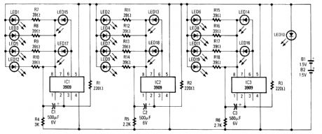
Three individual flashing circuits that use an LM3909 LED flasher/oscillator IC create the appearance of a pseudo-random firing order. The combination of C1/R4, C2/R5, and C3/R6 control the blink rate, which is between 0.3 and 0.8s, and the inherent wide tolerance range (-20% to +80%) of standard electrolytic capacitors add to the irregularities of the blink cycles. The continuous current drain is about 10 mA; however, if you decrease the values of R4 through R6 or C1 through C3 in order to increase the blink rate, the current will then increase proportionally.
Note in particular that extemal current-limiting resistors aren't needed for LED13 through LED18; the resistors are built into the ICs. LED10, which serves as the tree's star, is a special kind of flashing LED that blinks continuously at a fixed rate. (View)
View full Circuit Diagram | Comments | Reading(2990)
Flash_Signal_Alarm
Published:2009/6/17 0:32:00 Author:May
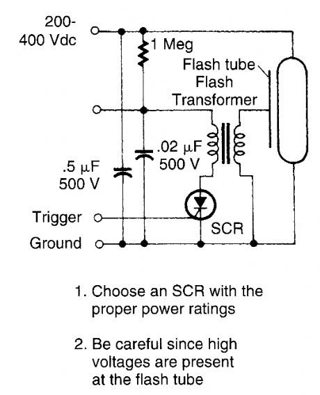
This circuit is useful if you need a low-energy flashing alarm. The 200 to 400-dc supply should have enough internal resistance to charge the 0.5 μF capacitor between flashes, about 2 or 3 time constants, which means about 500 kΩ to 1 MΩ for a 1-s rate. Use lower values for higher rates. (View)
View full Circuit Diagram | Comments | Reading(777)
LED_Flasher_for_2_to_10_LEDs
Published:2009/6/17 0:10:00 Author:May
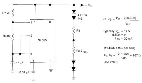
This LED flasher has double-ended output connection. The circuit can be used with 1 to 5 LEDs on each side as indicated. (View)
View full Circuit Diagram | Comments | Reading(742)
Super_LED_Flasher
Published:2009/6/17 0:07:00 Author:May
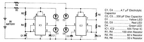
The super LED flasher is actually two complete LED flasher circuits on one circuit on one circuit board. The first LED flasher is made up of IC1 and LEDs D1 and D2. IC1 is a 555 timer IC configured as an astable (free-running) multivibrator with its output on pin 3.
The frequency of the 555's oscillation is controlled by R2, R3, and C1. Resistor R1 limits the input voltage to a low enough level to prevent damage to the IC. As the 555 IC oscillates, the output of pin 3 goes high (+) then low (-). When the output is high it supplies current to D1, which lights up.When it is low, pin 3 sinks current and D2 lights up. This happens because LEDs are polarity-sensi-tive (like all other diodes, they permit current flow in only one direction) and one lead of each LED has been connected to the respective polarity needed to light that LED.
The second LED flasher, made up of IC2 and LEDs D3 and D4, operates in the same way as the first LED flasher. (View)
View full Circuit Diagram | Comments | Reading(1725)
Dark-Activated_LED_Flasher
Published:2009/6/16 23:58:00 Author:May
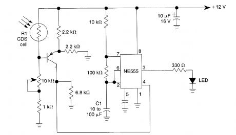
This circuit can be used as a small beacon or marker light, amd toys or novelty items. R1 is an LDR that has≥10 kΩ dark-resistance, or a CDS photocell. C1 determines the flash rate. (View)
View full Circuit Diagram | Comments | Reading(1097)
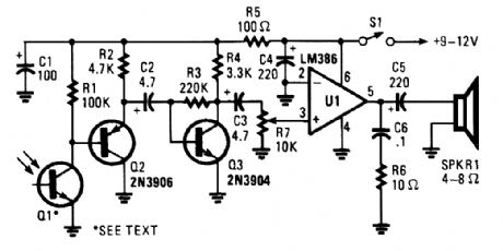
LIGHT_WAVE_VOICE_COMMUNICATION_RECEIVER
Published:2009/6/16 23:54:00 Author:May
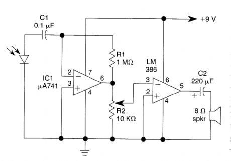
This light-wave receiver consists of a 741 op-erated as a preamplifier and an LM386 operated as a power amplifier. Potentiometer R2 is the gain control. Various kinds of detectors can be used as the front end of the receiver. Phototransistors are very sensitive, but they do not work well in the presence of too much ambient light. A 100-kQ se-ries resistor is required if you use a phototransis-tor. Solar cells, photodiodes, and LEDs of the same semiconductor as the transmitter all work well in this circuit. (View)
View full Circuit Diagram | Comments | Reading(986)
LED_Flashers
Published:2009/6/16 23:54:00 Author:May
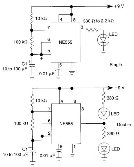
A 555 is used to switch an LED on and off. C1 determines the flash rate. Single ended (one LED) and double-ended (altemating) flashers are shown. (View)
View full Circuit Diagram | Comments | Reading(826)
LIGHT_WAVE_VOICE_COMMUNICATION_TRANSMITTER
Published:2009/6/16 23:54:00 Author:May


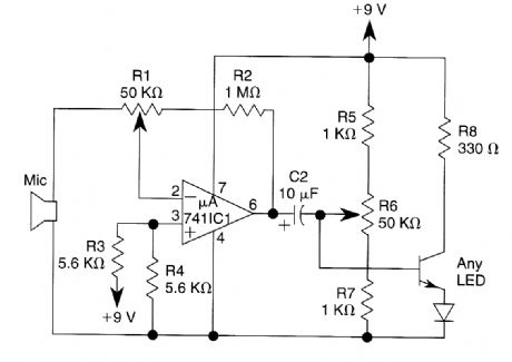
This transmitter uses a 741 op amp as a high-gain audio amplifier, which is driven by a rnicro-phone. The output of the 741 is coupled to Q1, which serves as the driver for a LED. Potentiometer RI is the amplifier's gain control. Miniature trimmer resistor R6 permits adjustment of the base bias of Ql for best transmitter performance. Gain control RI can be eliminated if C1 and R2 are con-nected directly to pin 2 of the 741. For maximum sensitivity, increase the value of R2 from 1 to 10MΩ and use a crystal microphone with a large diaphragm. (View)
View full Circuit Diagram | Comments | Reading(1125)
| Pages:1437/2234 At 2014211422142314241425142614271428142914301431143214331434143514361437143814391440Under 20 |
Circuit Categories
power supply circuit
Amplifier Circuit
Basic Circuit
LED and Light Circuit
Sensor Circuit
Signal Processing
Electrical Equipment Circuit
Control Circuit
Remote Control Circuit
A/D-D/A Converter Circuit
Audio Circuit
Measuring and Test Circuit
Communication Circuit
Computer-Related Circuit
555 Circuit
Automotive Circuit
Repairing Circuit