
Circuit Diagram
Index 1438
FM_LIGHT_BEAM_TRANSMITTER
Published:2009/6/16 23:52:00 Author:May
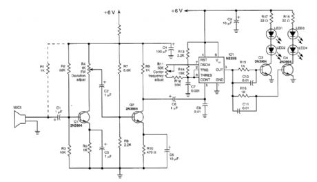
This transmitter uses two-stage amplifier Q1/Q2 to frequency modulate an NE555 (configured as a VCO) operating at about 50 kHz. The resultant FM-modulated pulse train is converted to light pulses via LED1 through LED4, driven by Q3 and Q4. (View)
View full Circuit Diagram | Comments | Reading(646)
FM_LIGHT_BEAM_RECEIVER
Published:2009/6/16 23:51:00 Author:May
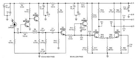
This receiver will pick up IR or light beams that are frequency modulated on a 50-kHz carrier Q2/Q1/Q3/Q4 from an active filter and amplifier and differential amp Q5/Q6 provide more gain. (View)
View full Circuit Diagram | Comments | Reading(806)
MODULATED_LIGHT_RECEIVER
Published:2009/6/16 23:48:00 Author:May
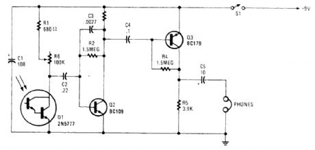
Using a phototransistor, this receiver will detect and demodulate a modulated light beam. R6 af-fects sensitivity. (View)
View full Circuit Diagram | Comments | Reading(2276)
36_LED_Flasher_Driver
Published:2009/6/16 23:48:00 Author:May
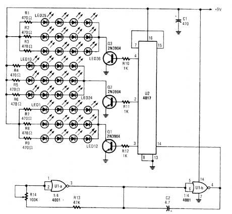
Originally intended as a 3-bell animation circuit for Christmas decorations, the circuit can be used for many other purposes that require a flasher of this kind. By re-connerting U2(see the data manual), more than three outputs can be be obtained. (View)
View full Circuit Diagram | Comments | Reading(1922)
MODULATED_LIGHT_TRANSMITTER
Published:2009/6/16 23:48:00 Author:May

A light-bulb filament can be modulated with audio as a method of optical transmission. Ampli-fier Q1/Q2/Q3 drives emitter-follower TR4. Adjust R10 for the Q point (light bulb) giving best results.It should have a filament with low thermal inertia for best audio responses. (View)
View full Circuit Diagram | Comments | Reading(791)
SIMPLE_LIE_DETECTOR
Published:2009/6/16 23:46:00 Author:May
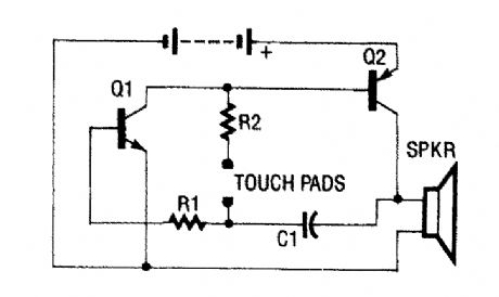
The circuit uses a two-transistor direct-coupled oscillator that has a frequency determined by C1, R2, and the (skin) resistance across the touch pads. Since C1 and R2 are fixed values, only the skin resistance across the touch pads can vary the sound of the oscillator. To sustain oscillations, C1 feeds a portion of the output from Q2 back to the input of Q1 through resistor R1.Transistor Ql is an npn type and transistor Q2 is a pnp type. The output of Q2 is fed into a small speaker. The circuit relies on the fact that the human skin conducts electricity.
C1 0.01-μF CapacitorQ1 2N3904 TransistorQ2 2N3906 TransistorR1 4.7kΩ ResistorR2 85kΩ Resistor (View)
View full Circuit Diagram | Comments | Reading(2998)
LASER_POWER_SUPPLY
Published:2009/6/16 23:39:00 Author:May
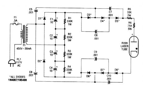
This supply generates an initial high voltage for ignition purposes. After ignition, the supply gen-erates about 1300 to 1500 V. If a higher ignition voltage (than the 6000 V supplied) is necessary, more multiplier stages can be added to D5 and D8. (View)
View full Circuit Diagram | Comments | Reading(2232)
FANTASTIC_SIMULATED_LASER
Published:2009/6/16 23:37:00 Author:May
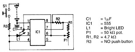
The circuit uses a 555 timer IC to power an ultrabright LED. The output is a pulsing red light that can be projected using lenses. An ultrabright Stanley LED, capable of 300-millicandle output, is tied to pin 3 of the 555 timer IC. That IC has been configured as an astable multivibrator. The fre-quency of this multivibrator is controlled by R1, R2, C1, and P1. You can vary the frequency by ad-justing P1, which changes the output from a slow blinking to a fast pulsating light. Resistor R3 is used to limit the current flowing into the circuit to a safe value, to prevent the LED and the IC from bum-ing out. Switch S1 applies power to the circuit when its button is pressed. (View)
View full Circuit Diagram | Comments | Reading(954)
HIGH_VOLTAGE_POWER_SUPPLY
Published:2009/6/16 23:37:00 Author:May
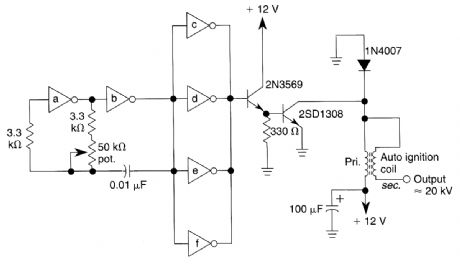
The high-voltage power supply is a CMOS-based oscillator that pulses a high-voltage ignition transformer. The transformer output is around 20 kV. (View)
View full Circuit Diagram | Comments | Reading(1628)
Sequential_Flasher
Published:2009/6/16 23:36:00 Author:May
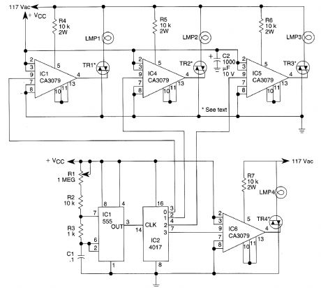
A 555 timer, IC1, drives a 4017 CMOS decade counter. Each of the 4017's first four outputs drives a CA3079 zero-voltage switch. Pin 9 of the CA3079 is used to inhibit output from pin 4, thereby disabling the string of pulses that the IC normally delivers. Those pulses occur every 8.3 ms, i.e., at a rate of 120 Hz. Each pulse has a width of 120 μs. Because of the action of the CA3079, the lamps connected to the triacs turn on and off near the zero crossing of the ac waveform. Switching at that point increases lamp life by reducing an inrush of current that would happen if the lamp were turned on near the high point of the ac waveform. In ad-dition, switching at the zero crossing reduces radio frequency interference (RFI) considerably. Cau-tion: The CA3079s are driven directly from the 117-Vac power line, so use care. (View)
View full Circuit Diagram | Comments | Reading(2971)
HANDHELD_LASER
Published:2009/6/16 23:35:00 Author:May
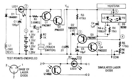
A laser diode TOLD9200 (Toshiba) is used as a source of laser light. Q3, Q2, and S1 form a touch switch to control the laser. L1 is an RF pickup coil to pick up energy from an RF-type battery charger.It is 10 tums of #18 wire on a 1/2 diameter. (View)
View full Circuit Diagram | Comments | Reading(1630)
LASER_POWER_SUPPLY_AND_STARTING_CIRCUIT
Published:2009/6/16 23:34:00 Author:May

This circuit delivers 10 kV peak, then limits current to 7.5 mA @ 2 kV. The resistors shown provide ballasting. The starting circuit cannot maintain the 10 kV under load and appears as a seriespass circuit with little drop in voltage. (View)
View full Circuit Diagram | Comments | Reading(741)
EFFICIENT_LASER_SUPPLY
Published:2009/6/16 23:32:00 Author:May

Driving Helium-Neon Lasers can be simplified considerably using this power-supply configura-tion. When power is applied, the laser doesn't conduct and the voltage across the 190-Ω resistor is zero. However, a resonant circuit and a voltage tripler then produces over 10 kV to turn on the laser. (View)
View full Circuit Diagram | Comments | Reading(1526)
NEGATIVE_ION_GENERATOR
Published:2009/6/16 23:31:00 Author:May
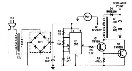
This oscillator-driver induces a high voltage in the windings of T2. (View)
View full Circuit Diagram | Comments | Reading(3178)
POWER_MOSFET_INVERTER
Published:2009/6/16 23:29:00 Author:May
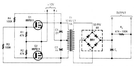
T1 is a suitable transformer for the voltage desired, with a 12.6-V CT winding. (View)
View full Circuit Diagram | Comments | Reading(1)
dc_to_ac_INVERTER
Published:2009/6/16 23:28:00 Author:May
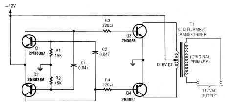
A multivibrator circuit drives a pair of 2N3055 power transistors transformer with a 120-V primary. (View)
View full Circuit Diagram | Comments | Reading(5817)
DIGITAL_INVERTER
Published:2009/6/16 23:27:00 Author:May
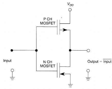
A CMOS digital inverter is formed by con-necting two MOSFETS, as shown. (View)
View full Circuit Diagram | Comments | Reading(855)
250_W_INVERTER
Published:2009/6/16 23:27:00 Author:May
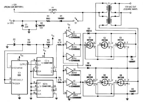
A 555 timer (IC1) generates a 120-Hz signal that is fed to a CD4013BE flip-flop (IC1-a), which divides the input frequency by two to generate a 60-Hz clocking frequency for the FET array (Q1 through Q6). Transformer T1 is a 12-/24-V center-tapped 60-Hz transformer of suitable size. (View)
View full Circuit Diagram | Comments | Reading(3619)
MICROCOMPUTER_TO_TRIAC_INTERFACE
Published:2009/6/16 23:16:00 Author:May
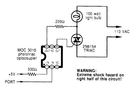
A microcomputer-to-triac interface uses a phototriac optoisolator to let safety-isolated logic sig-nals directly control high-power loads. Depending on the input waveforms and the load, this circuit can be used in either an on/off switch or a proportional phase control. A low input powers the lamp. (View)
View full Circuit Diagram | Comments | Reading(1845)
RECEIVER_INTERFACE_CIRCUIT_FOR_PREAMPS
Published:2009/6/16 23:05:00 Author:May
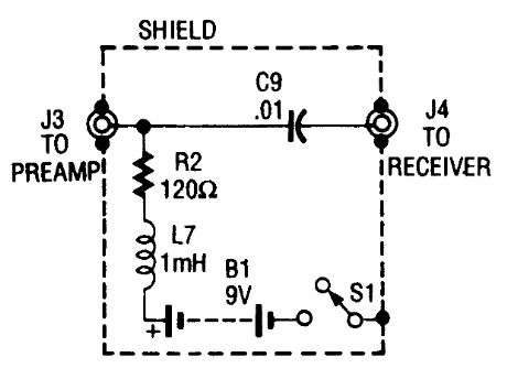
The purpose of the receiver/interface circuit is to pass RF to the receiver through capacitor C9, while adding dc power to the feedline through R2 and RF choke L7. (View)
View full Circuit Diagram | Comments | Reading(577)
| Pages:1438/2234 At 2014211422142314241425142614271428142914301431143214331434143514361437143814391440Under 20 |
Circuit Categories
power supply circuit
Amplifier Circuit
Basic Circuit
LED and Light Circuit
Sensor Circuit
Signal Processing
Electrical Equipment Circuit
Control Circuit
Remote Control Circuit
A/D-D/A Converter Circuit
Audio Circuit
Measuring and Test Circuit
Communication Circuit
Computer-Related Circuit
555 Circuit
Automotive Circuit
Repairing Circuit