
Circuit Diagram
Index 1423
VIDEO_LINE_DECODER_I
Published:2009/6/18 2:55:00 Author:May
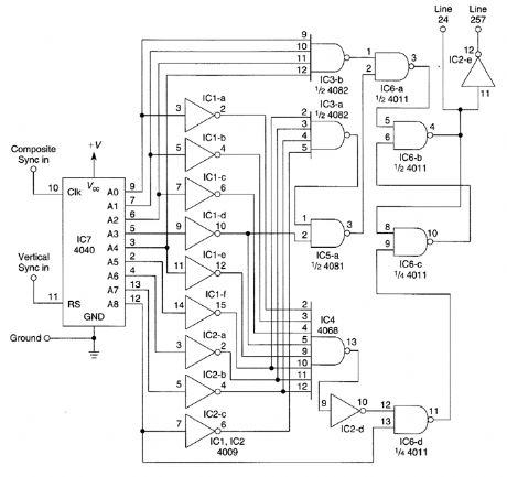
This line decoder uses only one pin for the line indicator. (View)
View full Circuit Diagram | Comments | Reading(865)
TRANSCEIVER_MEMORY_BACKUP
Published:2009/6/18 2:52:00 Author:May

Although designed for a Kenwood TR7730, this idea might be adapted to other transceivers. This circuit will retain the frequencies in memory while moving the rig from car to house and vice versa. When connected to an external power source, battery B1 is charged through R1 and D1.D1 prevents B1 from discharging when connected to an extemal supply that is tumed off. When extemal power is removed, D2 provides a current path to the TR-7730 to retain the memory's contents. However, the TR-7730 power switch should be tumed off before extemal power is removed because B1 will not provide power for normal operation. (View)
View full Circuit Diagram | Comments | Reading(882)
PTT_CONTROL_FROM_RECEIVER_AUDIO
Published:2009/6/18 2:51:00 Author:May
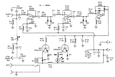
This system will key a transmitter or other device that can be keyed by a relay closure. Audio is amplified, limited, and is rectified and drives relay driver Q2 and LED indicator. The transmitter au-dio output was used to feed a keyed transmitter and can be deleted or ignored where this feature is unnecessary. (View)
View full Circuit Diagram | Comments | Reading(1633)
ONE_WATT_CW_TRANSMITTER
Published:2009/6/18 2:49:00 Author:May
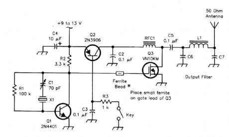
C6,C7 L1820 pF disc ceramic (160 meters) 33 turns,#30, T37-2 (160 meters) 470 pF disc ceramic (80 meters) 23 turns,#30, T37-2 (80 meters) 220 pF disc ceramic (40 meters) 17 turns,#30, T37-2 (40 meters) 150 pF disc ceramic (30 meters) 14 turns,#30, T37-2 (30 meters) 100 pF disc ceramic (20 meters) 12 turns,#30, T37-2 (20 meters) 82 pF disc ceramic (17 meters) 10 turns,#30, T37-2 (17 meters) (View)
View full Circuit Diagram | Comments | Reading(1371)
AUDIO_BREAKOUT_BOX
Published:2009/6/18 2:48:00 Author:May
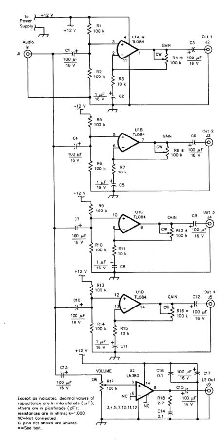
In many radio shacks, one receiver audio-output line feeds a multitude of add-ons, such as one or more TNXs, SSTV modems, PC plug-in boards, and, perhaps, speakers. Having to manually plug the audio source from one accessory to another is inconvenient, if not frustrating as well. Overload-ing the sources by connecting the loads in parallel isn't satisfactory, either.The audio breakout box takes the audio output from a receiver (or other audio source) and ap-plies it to the inputs of four identical, independent, low-level N' buffer/amplifiers and one high-level (1-W qutput) AI' channel. Each low-level output channel can provide up to 20 dB of gain that's in-dependently adjustable. (View)
View full Circuit Diagram | Comments | Reading(933)
TYPICAL_NE567_TONE_DECODER_CIRCUIT
Published:2009/6/18 2:47:00 Author:May
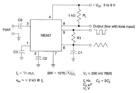
This circuit illustrates use of NE567 as a tone decoder. (View)
View full Circuit Diagram | Comments | Reading(2693)
FM_STEREO_DECODER
Published:2009/6/18 2:46:00 Author:May
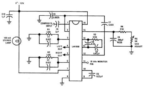
Using an LM1800, this circuit takes composite baseband MPX input and recovers L7R audio channels. The VCO is set for 19 kHz (or 15.7 kHz for TV applications) or as needed. (View)
View full Circuit Diagram | Comments | Reading(1203)
DTMF_DECODER
Published:2009/6/18 2:44:00 Author:May
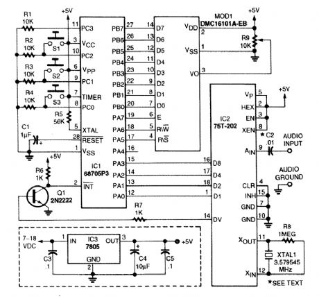
This DTMF decoder uses a Motorola 68705P3 microcontroller and a 75T202 DTMF receiver (Sil-icon Systems, Inc.). An LCD module is used for the display (MOD1). Switch S1 is used to scroll the display, S2 clears the display, and 53 clears the memory. (View)
View full Circuit Diagram | Comments | Reading(2678)
RF_SIGNAL_GENERATOR
Published:2009/6/18 2:42:00 Author:May
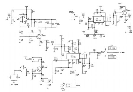
This circuit uses a VFO operating from 15 to 18 MHz (U1), which feeds a balanced mixer (U2). A fixed oscillator signal is mixed with this signal to generate an output from 0.4 to 33 MHz. FL1 and FL2 are low- and high-pass filters that are used to eliminate undesired mixer products. Amplifier U3/Q3 supplies up to 200 mV rms to the output jack. (View)
View full Circuit Diagram | Comments | Reading(2420)
65_MHz_VFO
Published:2009/6/18 2:40:00 Author:May
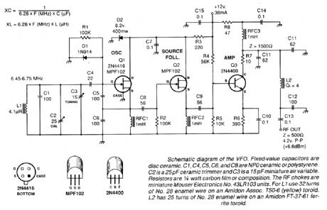
Fixed-value capacitors are disc ceramics. C1, C4, C5, C6, and C8 are NPO ceramic or polystyrene. C2 is a 25-pF ceramic trimmer and C3 is a 15-pF miniature air variable capacitor. The resistors are 1/4-W carbon film or composition. The RE chokes are miniature Mouser Electronics No. 43LR103 units. For L1, use 32 turns of #28 enamel wire on an Amidon Assoc. T50-6 (yeltow) toroid. L2 has 25 turns of #28 enamel wire on an Amidon Ft-37-61 ferrite toroid. (View)
View full Circuit Diagram | Comments | Reading(1252)
dc_to_dc_CONVERTER_II
Published:2009/6/18 2:40:00 Author:May
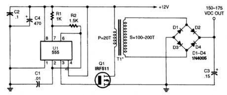


In this dc-to-dc converter, the 555 is used to produce a rising and collapsing field in TI's primary, generating a high voltage in TI's secondary winding. That voltage is then full-wave, bridge rectified by Dl through D4, and filtered by C3. T1 is an Amidon Associates EA-775-375E core and nylon bob-bin, with #26 wire for the primary and #28 or #30 for the secondary. About 5 W of power is available. (View)
View full Circuit Diagram | Comments | Reading(3894)
AUDIBLE_SWR_DETECTOR_ADAPTER
Published:2009/6/18 2:39:00 Author:May
This SWR detector audio adapter is designed specifically for blind or vision-impaired atrtateurs, but anyone can use it. Instead of using a meter (or meters) to indicate antenna system forward and reflected voltages, this adapter generates two tones with frequencies that are proportional to the re-spective voltages. The tones are fed to a pair of stereo headphones (the miniature types are ideal) so that one ear hears the forward-voltage tone and the other ear hears the reflected-voltage tone. Thus, tuning up a transmitter is simply a matter of tuning for the highest-pitched tone in the left ear and the lowest-pitched tone in the right ear. (View)
View full Circuit Diagram | Comments | Reading(878)
NEGATIVE_STEP_up_dc_to_dc_CONVERTER
Published:2009/6/18 2:37:00 Author:May
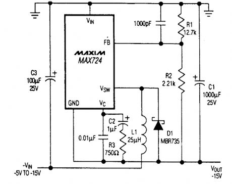
A Maxim MAX724 is used in a step-up switching converter to provide -15-V output from a-5-to-15-V input. (View)
View full Circuit Diagram | Comments | Reading(980)
PROGRAMMABLE_CW_IDENTIFIER_
Published:2009/6/18 2:37:00 Author:May
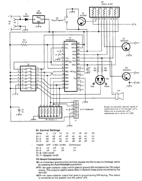
The identifier uses an MTA81010 microchip,containing a 1024-bit serial EEPROM and a rmcro-controlier It runs from a 9-V battery.A standard AT-type keyboard is used to progran the desiredmessage Speed varles from 5 to 25 wpm. (View)
View full Circuit Diagram | Comments | Reading(760)
ONE_CHIP_AFSK_GENERATOR__
Published:2009/6/18 2:34:00 Author:May
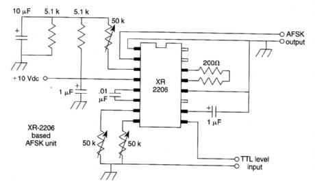
Built around an XR2206 IC,this circuit wiⅡ generate AFSK signals in the 1000- to 3000-Hz range
(View)
View full Circuit Diagram | Comments | Reading(2804)
IMPROVED_CW_TRANSMITTER_KEYING_CIRCUIT
Published:2009/6/18 2:32:00 Author:May


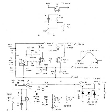
Typical (A) QRP keying circuit; (B) Improved QRP keying circuit with CMOS T/R keying control.Op amp U2b is a basic inverting amplifier with a gain of one. The capacitor C5 across the feedback resistor R11 makes it an integrator. The RC time constant of Rll and C5 determine the ramp time.The values shown will produce a 5-ms ramp. Use a good-quality capacitor for C5, such as a mylar or polypropylene type. A power transistor is placed inside the feedback loop so that the circuit can sup-ply several hundred milliamperes of current. Control P2 sets the stand-by output voltage as seen atthe emitter of Q1. U2a buffers the voltage from P2. This isolates the pot from the input of the inte-grator. With the key up, adjust the pot until you just start to see an output from your transmitter, then back it off a little. Typically, this will be between 2 and 4 V. Your output signal will now have the proper 5-ms leading and falling edges and there will be no delay between key closure and the start of the output signal.You must supply the op amp and collector of Q2 with at least 15 V to produce a full 12-V output on the emitter.Parts listR1,R4,R12 1kΩ1/4W C1 0.01μFdiskR2 47 kΩ1/4W C2 0.001μf' diskR3, R8, R11 100 kΩ C3, C4 10μF, 25VelectrolyticR6, R7 22 kΩC5 0.047μF poly-film typeR9 47Ω C6 1μF, 25 V electrolyticR10 10Ω C7 SkippedP1100 kΩ or 500 kQ trimpot C8 100 pF, 26 \I electrolyticP210 kΩ trimpot D1, D2 1N4148 diodeD3, D4, D5 1N4001 1-A diodeQ1 2N3904 NPNQ2 Tip 41-to-220 NPNU1 4011B CM0S NAND gatesU2 LM358 dual op amp (View)
View full Circuit Diagram | Comments | Reading(1497)
ULTRA_LOW_POWER_dc_to_dc_CONVERTER_FOR_PERSONAL_COMMUNICATIONS_PRODUCTS
Published:2009/6/18 2:30:00 Author:May


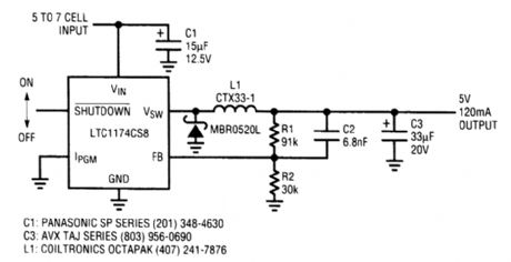
The LTC1174 step-down converter is designed specifically to eliminate noise at audio frequen-cies while maintaining high efficiency at low output currents. This circuit shows a 5-V, 120-mA out-put derived from 5 to 7 NiCad or NiMH cells. Small input and output capacitors that are capable of handling the necessary ripple currents help conserve space. In applications where shutdown is de-sired, this feature is available (otherwise short this pin to Vin).The LTC1174's internal switch, connected between Vin and Vsw is current controlled at a peak of approximately 340 mA. Low peak switch current is one of the key features that allows the LTC1174 to minimize system noise compared to other chips that carry significantly higher peak currents, eas-ing shielding and filtering requirements, and decreasing component stresses. Output current of up to 450 mA is possible with this device by connecting the 1 pgm pin to Vin. This increases the peak current to 600 mA, allowing for a high average output current. (View)
View full Circuit Diagram | Comments | Reading(876)
45_MHz_IF_AMPLIFIER_WITH_CRYSTAL_FILTER
Published:2009/6/18 2:29:00 Author:May
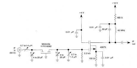
A 40673 dual-gate MOSFET is matched to a crystal filter at 45 MHz. The filter impedance is around 2kΩ. The + 4-V source can be made variable for gain control (about +4 to -4V.) (View)
View full Circuit Diagram | Comments | Reading(1206)
RF_PREAMPLIFIERS
Published:2009/6/18 2:27:00 Author:May
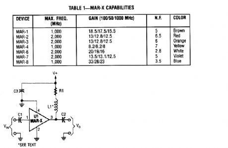
In this basic MAR-x-based circuit, both the input and output are comprised of a single dc-blocking capacitor (C1 and C2 for the input and output, respectively). The dc power-supply net-work (comprised of L1 and BI) is attached to the MAR-x via the RF-output terminal (lead 3). (View)
View full Circuit Diagram | Comments | Reading(993)
dc_to_dc_CONVERTER
Published:2009/6/18 2:26:00 Author:May
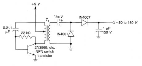
This converter should be useful where a few milliamperes of dc at a higher voltage than available supplies can deliver is needed. T1 is typically a 1 kΩ CT:10-kΩ transistor audio transformer. De-pending on T1, about 50 to 150 Vdc can be obtained at a few milliamperes. (View)
View full Circuit Diagram | Comments | Reading(111)
| Pages:1423/2234 At 2014211422142314241425142614271428142914301431143214331434143514361437143814391440Under 20 |
Circuit Categories
power supply circuit
Amplifier Circuit
Basic Circuit
LED and Light Circuit
Sensor Circuit
Signal Processing
Electrical Equipment Circuit
Control Circuit
Remote Control Circuit
A/D-D/A Converter Circuit
Audio Circuit
Measuring and Test Circuit
Communication Circuit
Computer-Related Circuit
555 Circuit
Automotive Circuit
Repairing Circuit