
Circuit Diagram
Index 1440
SIMPLE_IR_DETECTOR
Published:2009/6/16 22:12:00 Author:May
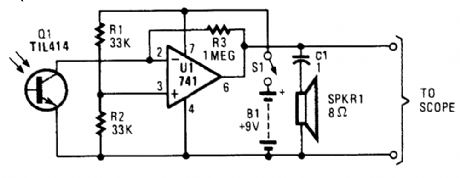
Useful for IR detection, this circuit uses an op amp of the 741 family (or similar) to detect and amplify IR pulses. (View)
View full Circuit Diagram | Comments | Reading(1531)
IR_CONTROLLED_REMOTE_A_B_SWITCH
Published:2009/6/16 22:11:00 Author:May
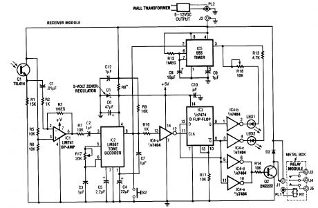
Useful for A/B control, the IR receiver shown controls a relay from an infrared beam that has a pulsed tone-modulated signal. Q1 is the photo receptor feeding op amp IC1, tone decoder IC2, and flip-flop IC3. IC5 turns off the indicator LEDs after about 15 seconds. (View)
View full Circuit Diagram | Comments | Reading(1190)
IR_PULSE_TO_AUDIO_CONVERTER
Published:2009/6/16 22:06:00 Author:May
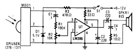
If your ear is good, you can use this IR-pulse-to-audio converter to troubleshoot infrared remote-controts. It is also a good project for detecting infrared-light sources. A photo cell module (Radio Shack P/N 276-137) detects IR radiation and drives audio IC U1. This circuit is useful for trou-bleshooting IR remote controls. (View)
View full Circuit Diagram | Comments | Reading(1207)
REMOTE_CONTROL_ANALYZER
Published:2009/6/16 22:05:00 Author:May
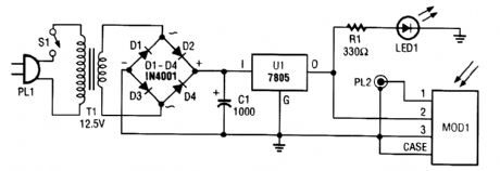
A schematic diagram for the remote analyzer is shown. The circuit is powered from a simple 5-V supply, consisting of PL1, 51, T1, abridge rectifier (comprised of Dl through D4), capacitor C1, and a common 5-V regulator, UI. Switch 51 is the on/off control and is optional. The power-supply trans-former used in the prototype is a 12.6-Vac unit, but any transformer that can supply at least 5.6-Vac will do. The 12.6-V unit was used solely because of its availability.The output of T1 is full-wave rectified by diodes Dl through D4 and filtered by C1. The bumpy dc output from the capacitor is regulated down to 5 V by UI, a 7805 integrated regulator, LED1 acts as a power indicator to let you know that the circuit is active.The 5-Vdc powers a GPIU52X infrared-detector module* (MODl), which demodulates the 40-kHz carrier used by most infrared remotes. After demodulation, the resulting logic pulses are sent to an oscilloscope via PL2, a BNC connector.
*Radio Shack part #276-137 (View)
View full Circuit Diagram | Comments | Reading(1013)
UNUSUAL_HALL_EFFECT_OSCILLATORS
Published:2009/6/16 22:01:00 Author:May
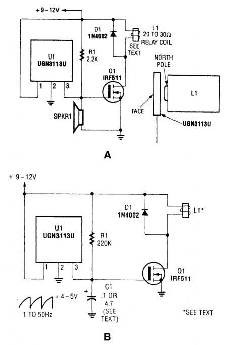
Although not intended for this application, Hall-effect switch can be used as the basis for a rather unusual oscillator. The oscillator can be reconfigured, as shown in Fig. B, to allow the circuit's oscillating frequency to be controlled via an RC network, comprised of RI and C1. (View)
View full Circuit Diagram | Comments | Reading(1687)
THE_TALKING_COMPASS
Published:2009/6/16 22:00:00 Author:May
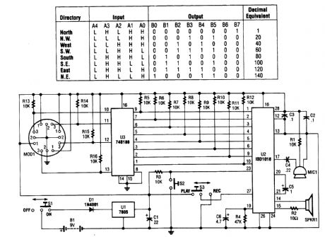
A talking compass is made up using a Hall-effect direction sensor (MOD1) and an ISD1016 analog audio storage device. It is possible to program eight two-second announcements, for each of the eight main compass directions.The Talking Compass is comprised of a digital compass (MOD1), and ISD1016 analog storage de-vice (U2), a 74S188 preprogrammed PROM (U3), and a handful of additional components. (View)
View full Circuit Diagram | Comments | Reading(1984)
GEIGER_COUNTER_Ⅱ
Published:2009/6/16 21:56:00 Author:May
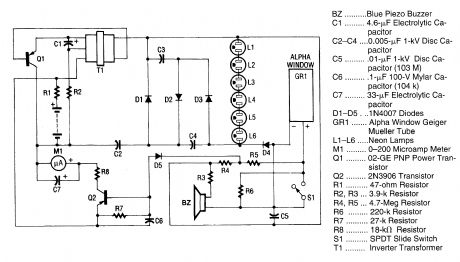
BZ..........Blue Piezo Buzzerc1......... 4.6-ptF Electrolytic CapacitorC2-04....0.005-μF 1-kV Disc CapacitorC5..........01-μF 1-kV Dtsc Capacitor (103 M)CG..........1-μF 100-V Mylar Capacitor (104 k)07......... 33-p.F Electrolytic CapacitorD1-D5....1N4007 DiodesGR1....... Alpha Window Geiger MuellerTubeL1-L6......Neon LampsM1......... 0-200 Microamp Meter Q1......... 02-GE PNP Power TransistorQ2......... 2N39O6 TransistorR1......... .7-ohm ReststorR2, R3,.. .3.9-k ResistorR4, R5.... 4.7-Meg ResistorR6......... 220-k ResistorR7......... .27-k ResistorR8.....,....18-kf) Resistor51.......... SPDT Slide SwitchT1......... InverterTransformer
Q1 is a pnp power transistor used in conjunction with a ferrite transformer to form a blocking-type oscillator. This oscillator is a fixed-frequency type, and the feedback to sustain oscillations is from capacitor C1. Because of the turns ratio of T1, the small ac voltage produced on its primary is converted to a large ac voltage on its secondary. That high-voltage ac is applied to the voltage trip-per stage, which consists of capacitors C2, C3, and C4 and diodes D1, D2, and D3. The resultant volt-age is now over 800 V and it is regulated by neon lamps L1 through L6. Diode D4 rectifies the high voltage and applies it to the cathode lead of the GM tube. The positive (+) bias on the GM tube is ap-plied to the anode by way of load resistors R4 and R5. Each time a radioactive particle strikes the GM tube, it causes the gas inside to ionize. This ionization of the gas creates a pulse, which drives the piezo speaker and is also coupled by diode D5 to the base of Q2. Transistor Q2 is a pnp type and is used to integrate the pulses in conjunction with capacitor C6. That produces a dc voltage level, which is in proportion to the quantity of pulses arriving at the base of Q2. The collector of Q2 is con-nected through resistor R8 to the (+) terminal of the meter. The other side of the meter goes directly to (-) of the battery. (View)
View full Circuit Diagram | Comments | Reading(2068)
GEIGER_COUNTER_I
Published:2009/6/16 21:51:00 Author:May
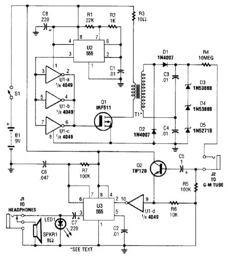
The circuit is built around a 4049 hex inverter (U1), a pair of 555 oscillator/timers (U2 and U3), two transistors, a Geiger-Muller tube, and a few additional support components. The first 555 (U2) is configured for astable operation. The output of U2 (a series of negative-going pulses) at pin 3 is fed to three parallel-connected inverters (U1-a, U1-b, and U1-c). The positive-going output pulses of the inverters are fed to the gate of Q1, causing it to toggle on and off.The output of Q1, which is connected in series with the primary of step-up transformer T1, pro-cluces a stepped-up series of pulses in T1's secondary. The output of T1 (approximately 300 V) is fed through a voltage doubler (consisting of D1, D2, C3, and C4), producing a voltage of around 600 V Three series-connected Zener diodes (D3, D4, and D5) are placed across the output of the voltage dou-bler to regulate the output to 500 V, fed through R4 (a 10-MΩ current-limiting resistor) and J2 to the anode of the GM tube. The limiting resistor also allows the detection ionization to be quenched.The cathode side of the tube is connected to ground through a 100-kΩ resistor, R5. When a par-ticle is detected by the GM tube, the gases within the tube ionize, producing a pulse across R5. That pulse is also fed through C5 and applied to the base of Q2 (a TIP120 npn transistor), where it is am-plified and clamped to 9V. The output of Q2 is inverted by gate U1-d, then it is used to trigger U3 (the second 555, which is configured for monostable operation). The output of U3 at pin 3 causes LED1 to flash, and produces a click that can be heard through speaker SPKR1 or headphones. The circuit is powered by a 9-V alkaline battery and draws about 28 mA when not detecting radiation. (View)
View full Circuit Diagram | Comments | Reading(1820)
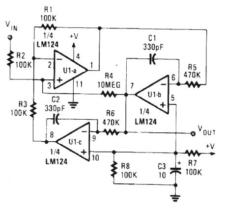
AND_GATE
Published:2009/6/16 21:46:00 Author:May
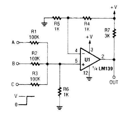
A left-over section of a quad op amp can be used to save cost and eliminate an extra logic chip for this AND gate. (View)
View full Circuit Diagram | Comments | Reading(0)
1_kHz_TONE_FILTER
Published:2009/6/16 21:29:00 Author:May
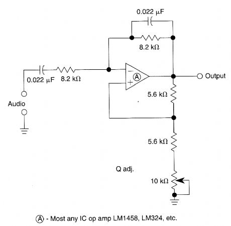


The Wien-bridge based filter has a variable bandwidth and a center frequency of 900 Hz. The circuit will oscillate if the 10-kΩ pot is set too low. (View)
View full Circuit Diagram | Comments | Reading(800)
FULL_WAVE_RECTIFIER_AVERAGING_FILTER
Published:2009/6/16 21:27:00 Author:May
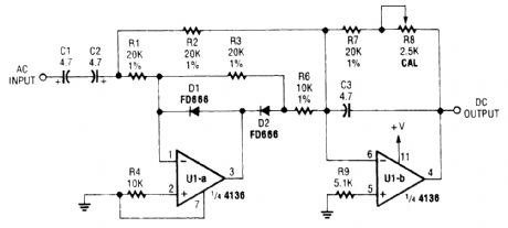
The input signal is rectified by D1 and D2 Op amp U1-a,and fed to output amp U2 R8 is set for correct circuit calibration. (View)
View full Circuit Diagram | Comments | Reading(770)
PASSIVE_T_FILTER_CONFIGURATIONS
Published:2009/6/16 21:19:00 Author:May
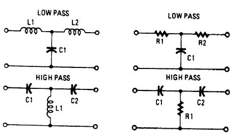
View full Circuit Diagram | Comments | Reading(817)
BI_QUAD_RC_BANDPASS_FILTER
Published:2009/6/16 21:19:00 Author:May
View full Circuit Diagram | Comments | Reading(702)
AUDIO_RANGE_FILTER
Published:2009/6/16 21:18:00 Author:May
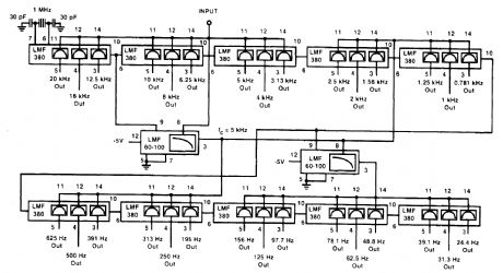
The LMF380 switched audio filter by National Semiconductor is used here to obtain a third-oc-tave filter set that covers the entire audio range. (View)
View full Circuit Diagram | Comments | Reading(773)
455_kHz_NARROW_BAND_IF_FILTER
Published:2009/6/16 21:14:00 Author:May
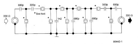
This filter uses five 455-kHz ceramic resonators. The impedance is 330Ω, the bandwidth is 800 Hz, and the ultimate rejection ≥60dB. The ceramic resonators could be replaced by crystals. (View)
View full Circuit Diagram | Comments | Reading(3280)
CURRENT_DRIVEN_SALLEN_KEY_FILTER
Published:2009/6/16 21:13:00 Author:May
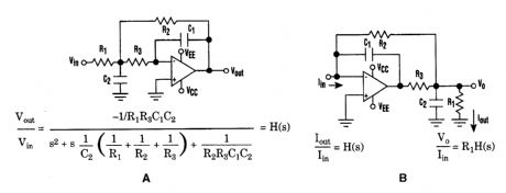
The low-pass Sallen-Key filter is staple for designers because it contains few components (A).By redesigning the filter, a current to voltage conversion can be avoided when the input signal to be filtered is in current form (B). (View)
View full Circuit Diagram | Comments | Reading(749)
SIMPLE_LOW_PASSLPACTIVE_FILTER_FOR_1kHz
Published:2009/6/16 21:12:00 Author:May
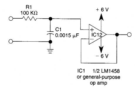
This simple filter uses an RC section for a filter element, with a voltage follower for other frequencies f3 dB = 1/6.28 R1C1 Response drops 6 dB/octave above f3 dB. (View)
View full Circuit Diagram | Comments | Reading(747)
SECOND_ORDER_LOW_PASS_FILTER_FOR_10_kHz
Published:2009/6/16 21:11:00 Author:May
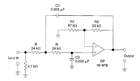
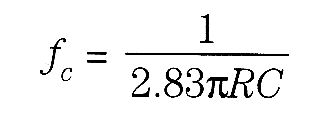
This circuit uses equal value capacitors, The cutoff frequency (fc) is (View)
View full Circuit Diagram | Comments | Reading(870)
EQUAL_COMPONEHNTS_SECOND_ORDER_HP_FILTER
Published:2009/6/16 21:10:00 Author:May
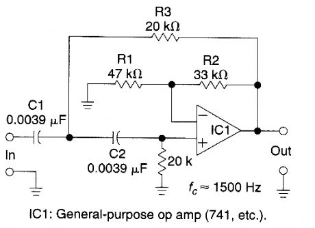

This filter circuit uses equal value components and is shown for 1500Hz.The values can be scaled for other frequencies.R=R1R2=2R1C=C1=C2 (View)
View full Circuit Diagram | Comments | Reading(726)
SIMPLE_HIGH_PASSHP_ACTIVE_FILTER_FOR_1_kHz
Published:2009/6/16 21:08:00 Author:May
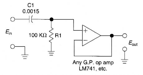
This simple 1kHz filter uses a voltage follower and an RCsection for a filter element,For other frequencies f3 dB-1/6.28 R1C1. The response drops 6 dB/octave below f3 dB. (View)
View full Circuit Diagram | Comments | Reading(811)
| Pages:1440/2234 At 2014211422142314241425142614271428142914301431143214331434143514361437143814391440Under 20 |
Circuit Categories
power supply circuit
Amplifier Circuit
Basic Circuit
LED and Light Circuit
Sensor Circuit
Signal Processing
Electrical Equipment Circuit
Control Circuit
Remote Control Circuit
A/D-D/A Converter Circuit
Audio Circuit
Measuring and Test Circuit
Communication Circuit
Computer-Related Circuit
555 Circuit
Automotive Circuit
Repairing Circuit