
Circuit Diagram
Index 1430
PRECISE_ONE_SHOT
Published:2009/6/17 21:28:00 Author:May
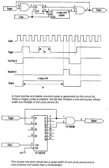
This approach uses a flip-flop, a shift register, and two gates (A). Before the one-shot pulse, the output of the NOR gate is 0. Consequently, the data input of the D-type flip-flop is equivalent to the trigger. When a trigger pulse is present, the flip-flop initiates the one-shot pulse, and the n-stage shift register controls the pulse width, tw , which is a multiple of the clock's period (B).The precision of the one-shot pulse is determined by the clock period, which is inversely pro-portional to its frequency. For the circuit to work properly, the width of the trigger pulse, twt, should be greater than one clock period.The OR gate masks the trigger's effect when the circuit is generating the desired pulse. The net result is a circuit that functions as a nonretriggerable rrtultivibrator.When the pulse needs to be only one-clock-period wide, the circuit can be simplified. All that's required are two D-type flip-flops and an AND gate. However, despite its simplicity, this circuit generates a more stable and precise one-shot pulse than a multivibrator. (View)
View full Circuit Diagram | Comments | Reading(1506)
LOGIC_PULSER
Published:2009/6/17 21:24:00 Author:May
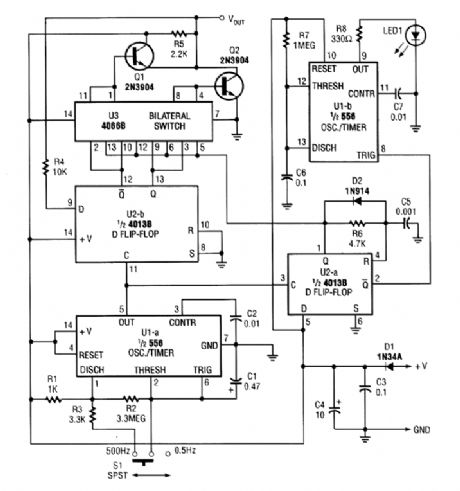
The logic pulser generates pulses at 500 Hz or 0.5 Hz. When the pulser's tip connects to an in-put that is already being driven high or low, the pulser senses the logic state and automatically pulses the input briefly to the opposite state. (View)
View full Circuit Diagram | Comments | Reading(3)
PULSE_GENERATOR
Published:2009/6/17 21:21:00 Author:May
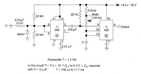
By using a 556 dual timer with IC1A acting as a waveshaper and IC1B as a pulse generator, a 10:1 range of pulse widths can be generated.A sine wave can be used to trigger this circuit. (View)
View full Circuit Diagram | Comments | Reading(3140)
ADD_ON_PULSE_GENERATOR
Published:2009/6/17 21:20:00 Author:May
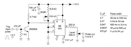
This pulse generator can supplement a standalone pulse generator. Using a transistor and a 555 Limer, pulse widths of <5 μs to 500 μs can be produced. The value of C3 is approximately found from Lhe formula:C3μF ≈ 1.1 x 10⁻⁵T whereT is the shortest pulse width (μs) desired in a 10:1 range(T should be greater than 5 μs)The capacitor values and consequent pulse width range are shown. (View)
View full Circuit Diagram | Comments | Reading(789)
PROXIMITY_ALARM_II
Published:2009/6/17 21:10:00 Author:May
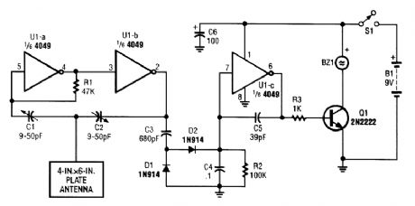
A CMOS logic gate is used to make up this circuit. When an object is near the antenna, the change in oscillator output is detected by D1 and D2 and amplified by U1C, which drives Q1, sound-ing alarm BZ1. (View)
View full Circuit Diagram | Comments | Reading(880)
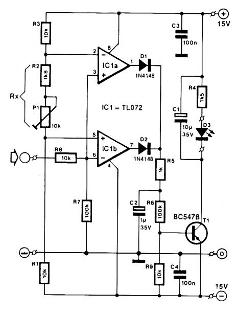
PROXIMITY_ALARM_I
Published:2009/6/17 21:08:00 Author:May
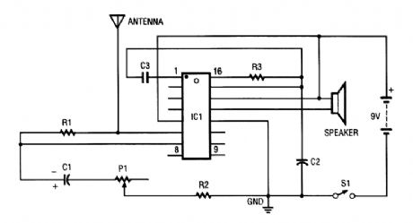
IC1 contains several oscillators and an amplifier. The low-frequency audio-signal oscillator is used to supply an input to the amplifier. That signal is the audio tone that is amplified, then supplied to the speaker by the amplifier.The high-frequency oscillator is purposely set to be very unstable. It is dormant or off until the resistor-capacitor (RC) network is changed. The resistance (fi) in this case is made up of R2 and P1. As the resistance of Pl is decreased, the unit becomes more sensitive (more unstable), and less ca-pacitance (C) is needed to cause the oscillator to oscillate.The capacitance required is provided by C2 and by any capacitance introduced via the antenna loop. When you come near that loop, your inherent body capacitance causes the high-frequency os-cillator to begin to oscillate, which then causes the low-frequency oscillator to be switched on in-ternally. Once the alarm is sounding, the IC is designed so that it latches , that is, it stays on until the power to it is switched off.C1 1-pFAxialCapacitorC2 27-pF Silver Mica CapacitorC3 0.1-pF Mylar CapacitorIC1 CM1001N ICP1 50-kQ Trimmer ResistorR1 75-kQ ResistorR2 200-Q ResistorR3 100-kQ ResistorS1 SPDT SwitchSpk Small SpeakerMisc IC Socket, Battery Snap, Ground Plate, Wire, PC Board (View)
View full Circuit Diagram | Comments | Reading(837)
SIMPLE_SAFETY_CIRCUIT
Published:2009/6/17 21:05:00 Author:May
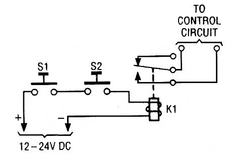
The simple two-hand safety-control switch shown here is little more than two pushbutton switches connected in series; both must be de-pressed in order to energize the relay. (View)
View full Circuit Diagram | Comments | Reading(1064)
LOUDSPEAKER_PROTECTOR
Published:2009/6/17 21:04:00 Author:May
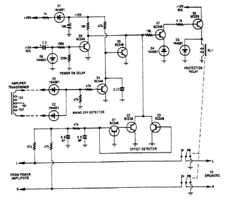
Transistors Q1, Q2, and Q3 monitor the two outputs of the stereo amplifier. If the offsets exceed ±2 V, Q7 is turned off, which turns off Q8 and the normally on relay. Diodes D2 and D5, together vith Q4, provide a mains voltage monitor. As soon as the ac input voltage disappears, as when the ampli-fier is turned off, Q4 turns off and Q5 turns on. This turns off Q7, Q8, and the relay. Hence, the loud-speakers are disconnected immediately after the amplifier is turned off. (View)
View full Circuit Diagram | Comments | Reading(914)
EAR_PROTECTOR
Published:2009/6/17 21:02:00 Author:May
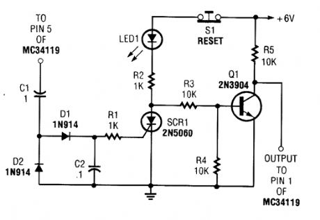
The ear protector is actually a peak audio- detector/shutdown circuit that disables the amplifier through its chip-disable input when the output volume of an amplifier reaches the set level. The cir-cuit, although intended for the MC34119 amplifier, should work with similar IC devices or applications. (View)
View full Circuit Diagram | Comments | Reading(868)
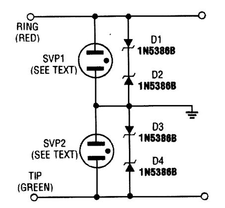
MODEM_FAX_PROTECTOR_FOR_TWO_COMPUTERS
Published:2009/6/17 21:01:00 Author:May
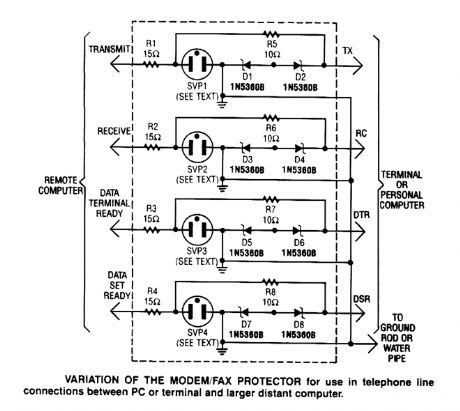
This modem/fax protector can be used in telephone-line connections betweenaPC or a terminal and a distant computer. In this circuit, the SVPs (surge voltage protectors) are at 230V.A good ground is a must for effective operation. (View)
View full Circuit Diagram | Comments | Reading(1224)
TIMED_SAFETY_CIRCUIT
Published:2009/6/17 20:57:00 Author:May
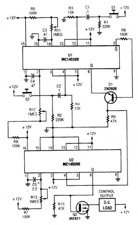
When S1 is closed, pin 9 of U1 goes low, turning on Q1 for a preset period. If S2 is closed during this period, Q2 is turned on for a preset period. R11 and R13 set the two time periods. (View)
View full Circuit Diagram | Comments | Reading(619)
OVERVOLTAGE_PROTECTION_CIRCUIT
Published:2009/6/17 20:55:00 Author:May
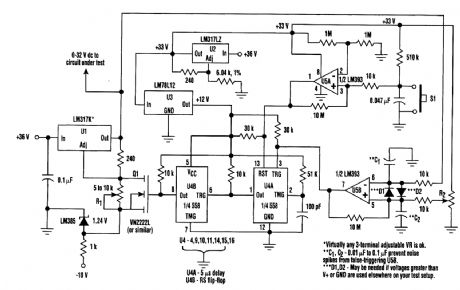
When testing a circuit, a source of voltage that is variable and has overvoltage shutdown is very useful. In this circuit, R1 is adjusted to 1 to 2 V below the eventual shutdown threshold. R2 sets the trip voltage. When this voltage is reached, the circuit shuts the voltage to the circuit under test down. To reset, reduce R1 below trip threshold and depress reset switch S1. (View)
View full Circuit Diagram | Comments | Reading(404)
MODEM_PROTECTOR
Published:2009/6/17 20:51:00 Author:May
This protector uses surge voltage protectors rated at 230-V breakdown. An effective ground should be used. (View)
View full Circuit Diagram | Comments | Reading(1052)
RELAY_FUSE_FOR_POWER_SUPPLIES
Published:2009/6/17 20:45:00 Author:May
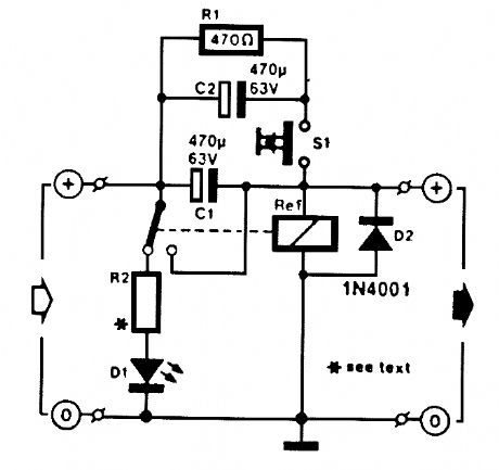
A method of adding overload protection to a power supply using a relay is shown. In each cir-cuit, the relay must be reset by a momentary switch using a charge on capacitor C2. This prevents overload ifthe short still exists. (View)
View full Circuit Diagram | Comments | Reading(1243)
OVERLOAD_INDICATOR
Published:2009/6/17 20:42:00 Author:May
Two op amps are used as comparators to indi-cate excessive magnitude of an AP signal, either positive or negative, even if the signal is asymmet-rical. P1 sets the reference voltage for both op amps. This circuit is useful for audio-amplifier and op-amp circuits using split power supplies. (View)
View full Circuit Diagram | Comments | Reading(1393)
SAFETU_CIRCUIT
Published:2009/6/17 20:41:00 Author:May
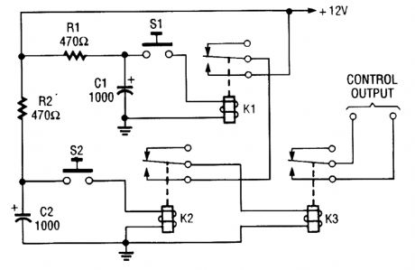
Because of the finite hold-on time of delay circuits R1/C1 and R2/C2, both S1 and S2 must be pressed at the same time to power up the load. (View)
View full Circuit Diagram | Comments | Reading(691)
ELECTRONIC_FUSE
Published:2009/6/17 20:39:00 Author:May
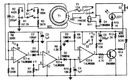
Basically, this circuit is an adjustable electronic circuit breaker, containing a toroidal transformer Lhat senses 60-Hz load current. T1 has a two-turn winding for primary, and 100 turns of #30 gauge wire for the secondary. A high-low range switch selects 0.1 to 6 A or 1 to 12 A. The primary winding of T1 carries fuL load current and voltage; should be suitably insulated, as should be RY1. (View)
View full Circuit Diagram | Comments | Reading(5)
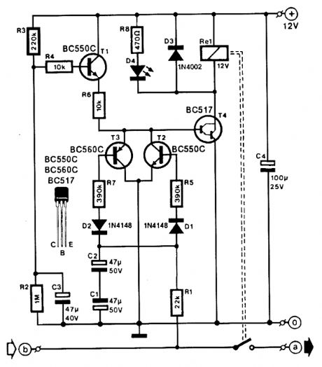
SPEAKER_PROTECTOR
Published:2009/6/17 20:36:00 Author:May
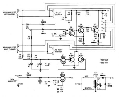
Most of the transistors in this speaker protector function as switches. Normally, Q4, Q5, and K1 are on and the speakers are connected to the amplifier. However, if a large dc voltage appears at an amplifier output, either Q3, or Q1 and Q2 turn on; biasing Q4 off. That action turns Q5 off, de-ener-gizes the relay, and disconnects the speakers from the amplifier. Components D1, D2, and Q6 form the overdrive-protection circuit. (View)
View full Circuit Diagram | Comments | Reading(4303)
dc_dc_CONVERTER_CIRCUIT_WITH_33_V_AND_5_V_OUTPUTS
Published:2009/6/17 4:35:00 Author:May
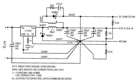
Input voltages can range from 8 V to 30 V. The load range on the 5 V is 0.05 A to 5 A while the 3.3-V load range is 0.1 A to I A. The circuit is self-protected under no-load conditions. Over all load and line conditions, including cross regulation, the 3.3-V output varies from 3.25 V to 3.27 V. The 5-V output varies from 4.81 Y to 5.19 V under the same conditions.In a typical application to 0.5 A on the 3.3 V and 0.25 A on the 5 V, efficiency is typically 76%. With an input voltage of 30 V and a full-load condition, the efficiency drops to 66%. In normal oper-ating regions, efficiency is always better than 70%. The 5-V ripple is less than 75 mV and the 3.3-V ripple less than 50 mV over all line and load conditions. (View)
View full Circuit Diagram | Comments | Reading(960)
TEMPERATURE_COMPENSATED_ONE_QUADRANT_LOGARITHMIC_CONVERTER
Published:2009/6/17 4:33:00 Author:May
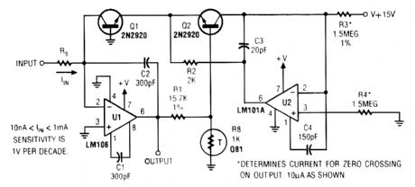
A logarithmic converter used to produce an output voltage that is proportional to the logarithm of an input current is shown. RS is the input impedance of the input source. (View)
View full Circuit Diagram | Comments | Reading(681)
| Pages:1430/2234 At 2014211422142314241425142614271428142914301431143214331434143514361437143814391440Under 20 |
Circuit Categories
power supply circuit
Amplifier Circuit
Basic Circuit
LED and Light Circuit
Sensor Circuit
Signal Processing
Electrical Equipment Circuit
Control Circuit
Remote Control Circuit
A/D-D/A Converter Circuit
Audio Circuit
Measuring and Test Circuit
Communication Circuit
Computer-Related Circuit
555 Circuit
Automotive Circuit
Repairing Circuit