
Circuit Diagram
Index 1432
VISUAL_CONTINUITY_TESTER
Published:2009/6/17 3:58:00 Author:May
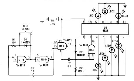
By judging the rate at which a particular LED flashes, you'll be able to estimate the resistance.The circuit consists of two IC's (1 4011 CMOS quad 2-input NAND gate, UI; and a 4024 binary counter, U2), seven LEDs, and a handful of additional components. All of the gates in UI are wired as inverters.Two of the inverters (U1-a and UI-b) comprise an astable-multivibrator (free-running oscillator) circuit, whose operating frequency depends on the amount of resistance detected between the test probes. Feedback from the output of the oscillator (at pin 4 of U1-b) back to the input of the circuit (at U1-a, pins 1 and 2) is provided via C1. Resistor, RI, along with the unknown resistance between the test probes, completes the RC timing circuit. The frequency of the oscillator decreases as the re-sistance between the test probes increases.The output ofthe oscillator is fed to pin 12 and 13 of UI-c, the output of which then divides along two paths. In the first path, UI-c's output is applied to the clock input of U2 (a 4024 binary counter) at pin 1; in the other path, the signal is fed through D2 and across capacitor C2, causing it to begin charging. The charge on C2 is applied to UI-d at pins 8 and 9. The output of that inverter (UI-d) is fed to the reset terminal (pin 2) of U2. If there is continuity or a measurable resistance between the test probes, U2's reset terminal is pulled low, triggering the counter and allowing it to process the in-put pulses (count).The rate of the count is proportional to the resistance between the test probes. If the resistance between the test probes is low, the counter advances slowly. The counter provides a 7-bit binary out-put that is wired to seven LEDs.When the test probes are placed across a short circuit, LED7 flashes. If the tester is placed across a resistance of, for example, 2 MO, LED1 will flash. In either case, the LED whose assigned value most closely corresponds to the resistance connected between the two probes will flash con-tinually 1t a steady pace, u|hile the other LEDs will seem to flash intermittently. (View)
View full Circuit Diagram | Comments | Reading(3850)
DIGITAL_TO_ANALOG_CONVERTER
Published:2009/6/17 3:56:00 Author:May
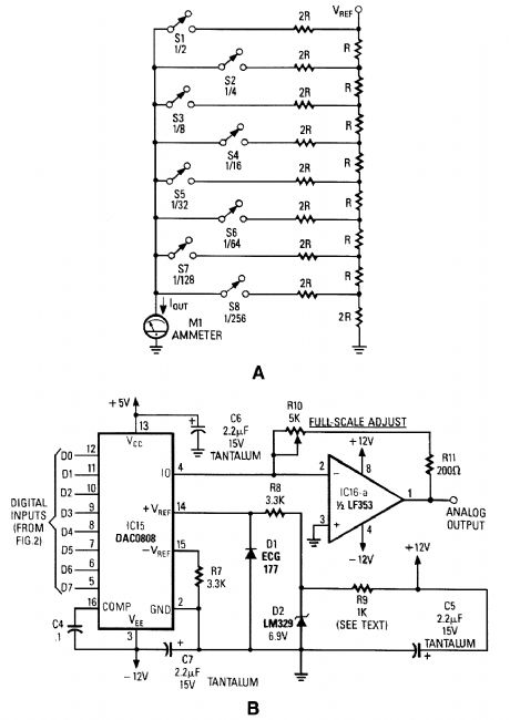

Figure A is an R/2R resistor ladder. Each switch that is closed increases the amount of current at Iout. A simple channel A/D converter is shown in Fig. B. The voltage reference (D2) is common to all channels, but the value of the dropping resistor (R9) varies as the number of DACs installed in the system. IC15 is a DAC0808 A/D converter chip. IC16A is an op amp to interface the output current from the D/A convert to an analog voltage output. (View)
View full Circuit Diagram | Comments | Reading(1197)
WATCH_TICK_TIMER
Published:2009/6/17 3:56:00 Author:May

This circuit adapts a frequency counter to measure intervals. It was originally used as a shutter speed checker for a photo ap-plication. The watch ticks are clipped and shaped and formed into a square wave. This square wave is used to gate an accurately known clock (1-MHz TTL XTAL OSC) and an external counter is used to directly count the clock pulses during the interval to be measured. A 1-MHz clock can be used to measure to a resolution of 1 psec. Accuracy = ± time base ±1 μs ±t1 count LSB. (View)
View full Circuit Diagram | Comments | Reading(824)
SIMPLE_WWV_CONVERTER_FOR_AUTO_RADIOS
Published:2009/6/17 3:54:00 Author:May
This simple frequency converter mixes the 15-MHz WWV/WVH signal with a 16-MHz signal from the LO to convert it down to 1 MHz so that it can be heard on AM-band receiver. (View)
View full Circuit Diagram | Comments | Reading(943)
3_A_dc_dc_CONVERTER_NEEDS_NO_HEATSINK
Published:2009/6/17 3:53:00 Author:May
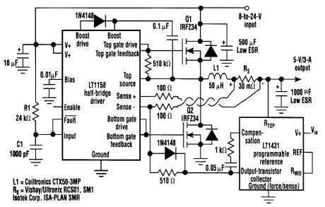
This regulator delivers 90% efficiency at 12-V input, 5-V output. It uses an LT1158 and LT1431 by Linear Technology, Inc. High efficiency is obtained by synchronously switching two power MOS-FETs in a step-down switching regulator. The LT1431 voltage reference combines with the LT1158 half-bridge driver to form a constant off-time current mode loop. (View)
View full Circuit Diagram | Comments | Reading(1539)
HARMONIC_DISTORTION_ANALYZER
Published:2009/6/17 3:52:00 Author:May
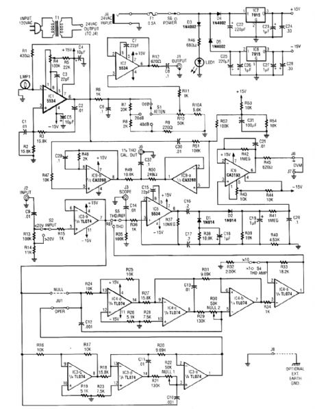
The circuit includes a low-distortion, 1-kHz oscillator and will measure THD at a user selected voltage level for voltage amplifiers, or for checking amplifiers of power levels to 600 W. It will detect THD levels of.005% (-86 dB). A built-in one-percent THD calibrator is included. The output device is a digital multimeter (DMM). (View)
View full Circuit Diagram | Comments | Reading(1670)
ELECTRONIC_SLOT_MACHINE
Published:2009/6/17 3:50:00 Author:May
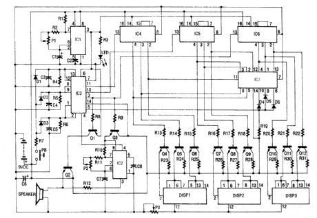
The slot machine's realistic action is provided by seven ICs and three displays, as shown. Two 555 CMOS timer ICs ge;terate pulses. IC1 is used to generate the clock pulses for the entire electronic slot machine. The pulses are coupled from the output (pin 3) to the clock inputs of IC4, IC5, and IC6, the display-driver ICs.
The displays are common-cathode 7-segment LED types. They are wired to display three different symbols, an L, a 7, and bar. When all three displays show the same symbols, IC7 (a 4023 triple 3-input NAND gate) decodes a winner and sends a signal to pin 5 of IC3. That IC is a 4001 CMOS NOR gate and it turns on IC2, a 555 timer IC. IC2 actually produces the winner tone on its output, pin 3.
Transistors Q4 through Q12 are used to drive the common-cathode displays. An LED is used to indicate the clock pulses, and a variable resistor is provided for each of these functions. Trimmer resistor PI controls the overall clock rate, P2 controls the winner tone, and P3 controls the display brilliance. (View)
View full Circuit Diagram | Comments | Reading(3474)
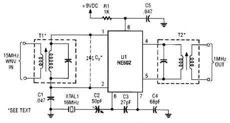
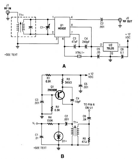
HIGH_PERFORMANCE_SHORTWAVE_CONVERTER
Published:2009/6/17 3:48:00 Author:May
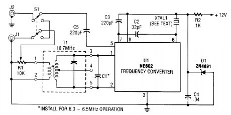
The NE602 chip, U1, contains oscillator and mixer stages. The mixer combines the oscillator sig-nal with the input RE signal to produce signals whose frequencies are the sum and difference of the input frequencies. For example, an 8.5-MHz oscillator and a 10-MHz incoming signal will give output signals at 18.5 MHz (10 + 8.5) and 1.5 MHz (10 - 8.5). Recall that 1.5 MHz is 1500 kHz and an ordinary AM radio will tune to it.The choice of crystal depends on what shortwave band you want to hear. The 9.5- to 10-MHz band is less crowded and includes the time-signal station WWW. For that band, you'll need a crystal of 8.5 to 8.9 MHz. There is no standard microprocessor crystal in that range, but you can use an am-ateur radio crystal, have a crystal custom-made, or use a CB crystal.Transformer T1 rejects signals that are outside the band you are interested in. Transformer T1 should pass signals from 9 to 11 MHz and attenuate all others. The transformer, T1, used in the circuit is a 10.7-MHz IF transformer salvaged from an FM radio.They are fairly easy to obtain new from parts stores and mail-order houses. Most 10.7-MHz IF trans-formers will tune across the 9.5- to 10-MHz band without modification; all you need to do is turn its tuning slug. To receive the 6.0- to 6.5-MHz shortwave band, you'll have to add a 150-pF capacitor. (View)
View full Circuit Diagram | Comments | Reading(1569)
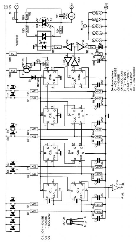
QUIZ_MASTER
Published:2009/6/17 3:46:00 Author:May
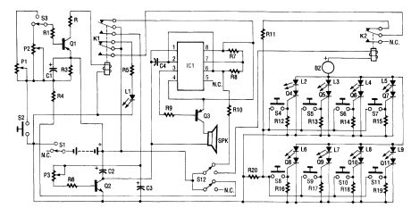
Up to eight players each have their own answer button to press, corresponding to the four Red Team and four Green Team LEDs on the master control board. As soon as the first contestant who thinks that he knows the answer presses the button, a loud tone sounds, all other contestants are locked out, and the contestant's indicator LED lights on the control board so that it's obvious who buzzed in first.
The control board also features two selectable time out periods-each adjustable from 3 to 15 seconds, setting specified time intervals in which the player must answer before the time's up! tone sounds. Eight SCRs form the heart of the circuit. The anode of each SCR has a positive (+) bias on it by way of an LED and a negative (-) bias on each cathode. As soon as a contestant depresses his or her switch button (S4 through S11), a positive bias is applied to the respective SCR gate. That bias latches the contestant's SCR on, which in tum lights up the appropriate LED on the master control board. At the same tirne, the activity of the SCR latching on turns on the answer buzzer (BZ) and locks out all other contestants. The lockout occurs because relay K2 contacts operate to remove the availability of a bias voltage to the gate of the other SCRs.
The other circuitry consists of a timer circuit and a time's-up tone-generating circuit. The timer circuit consists of transistor Q1, capacitor C1, resistors R1 through R3, and trimmer resistors P1 and P2. Depending on the adjustment of the trimmer resistors and selection switch S3, a specific time period can be set. The time's-up tone-generating circuit is made up of IC1, transistors Q2 and Q3, and the associated resistors and capacitors. The on time of the tone can be set by P3. Relay K1, which is operated by the timer circuit, serves to reset the entire unit for the next question. (View)
View full Circuit Diagram | Comments | Reading(2026)
ONE_CHIP_CRYSTAL_CONTROLLED_CONVERTER
Published:2009/6/17 3:42:00 Author:May
The circuit can work over a wide range of frequencies. XTAL 1 is a fundamental-frequency crystal. T1 and C1 are tuned to the input frequency. An application of this circuit is a simple shortwave converter for AM radios, etc. A tuneable oscillator can also be used, as shown. (View)
View full Circuit Diagram | Comments | Reading(1062)
ELECTROMAGNETIC_RING_LAUNCHER
Published:2009/6/17 3:40:00 Author:May
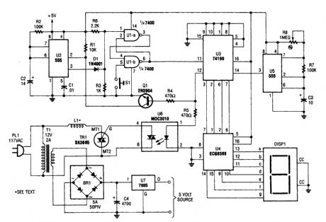
The electromagnetic ring launcher is comprised of four subcircuits: a clock circuit (built around U5, a 555 oscillator/timer configured for astable operation), a count-down/display circuit (built around U3), a 74190 synchronous up/down counter with BCD outputs that is configured for countdown operation; U4, a ECG8368 BCD-to-7-segment latch/decoder/display driver; and DISP1, a commnon-cathode seven-segment display), a trigger circuit (comprised of U6), an MOC3010 optoisolator/coupler with Triac-driver output; TRI, an SK3665 200-PIV, 4-A Triac; and a few support components), and a reset circuit (comprised of U1, a 7400 quad 2-input NAND gate; U2, a second 555 os-cillator/timer configured for monostable operation; and a few support components).
This circuit is that of a repulsion coil (L1) used to demonstrate the principle of electromagnetic repulsion by propelling a metal ring around the core of L1 through the air. A countdown circuit is provided to count seconds before launch. (View)
View full Circuit Diagram | Comments | Reading(6015)
DUAL_CONTROL_SWITCH_USES_ac_SIGNALS
Published:2009/6/17 3:37:00 Author:May
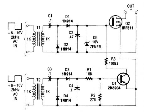
The Dual-Control Switch uses two 6-10-Vac sources to trigger the circuit on and off; one source for each function. (View)
View full Circuit Diagram | Comments | Reading(780)
SIMPLE_ac_VOLTAGE_CONTROL
Published:2009/6/17 3:34:00 Author:May
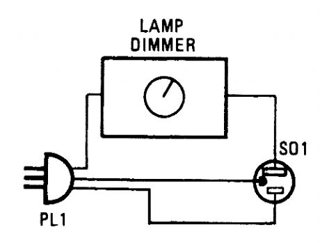
Lamp dimmers can be used for more than just controlling lights. Just provide one with an ac line cord and a socket, and discover just how useful they can be. (View)
View full Circuit Diagram | Comments | Reading(692)
ENERGY_CONSUMPTION_MONITOR
Published:2009/6/17 3:34:00 Author:May
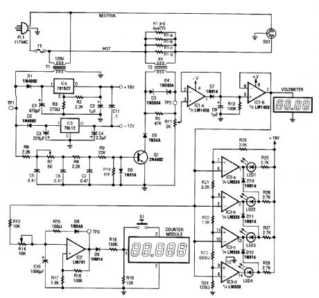
The EOM circuit consists of four sections, as shown in the block diagram. A power converter generates a voltage that is proportional to the true of real power consumed by the load. That voltage feeds both a bargraph and a voltage-to-pulse converter. The bargraph gives an approximate indication of the amount of power used, and the voltage-to-pulse converter produces a pulse whose frequency is proportional to the power. The pulse triggers the counter module, which displays the cost of powering the monitored load. (View)
View full Circuit Diagram | Comments | Reading(925)
SIMPLE_POWER_DOWN_CIRCUIT
Published:2009/6/17 3:33:00 Author:May
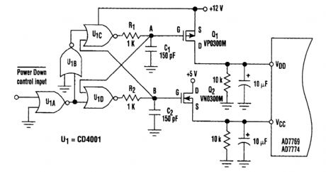
This circuit adds a power-down function to analog I/O ports (for example, the AD7769 and AD7774). Moreover, the diodes ordinarily needed to protect the devices against power-supply mis-sequencing can be eliminated (see the figure).In the circuit, MOSFETs Q1 and Q2 switch the +5- and +12-V supplies, respectively, in a se-quence controlled by two cross-coupled CD4001 CMOS NOR gates (U1C and U1D). The sequence in which power is applied is important: The controlled circuits may be damaged anytimeVCC exceeds VDD + 0.3 V. Consequently, the NOR gates must be powered from a 12-V supply throughout the power-down sequence.Bringing the power down control high (+5 V) applies power to the controlled circuit by turning on all MOSFETs. Specifically, raising the power down brings the output of U1C low, causing capaci-tor C1 to discharge VOL exponentiallywith time constant R1C1. As the voltage on C1 falls, two events occur. First, it puts a negative gate-source voltage on P-channel Q1, turning it on.Second, it causes output gate U1D to go high. With the output of U1D high, capacitor C2 charges exponentially to VOH-about 12-V-applying a positive gate-source voltage to turn on Q2. In the power down mode, the Power Down control is brought low and the RC circuits and their delays work in reverse. Consequently, capacitor C2 discharges to the logic input of U1C before C1 can charge. Hence, Q2 turns off before Q1. (View)
View full Circuit Diagram | Comments | Reading(1108)
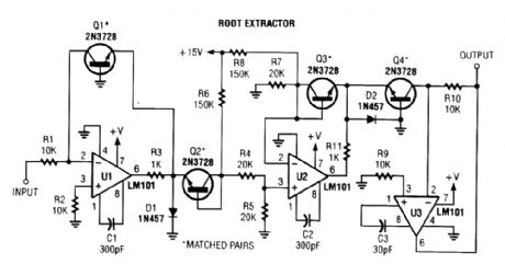
ROOT_EXTRACTOR
Published:2009/6/17 3:29:00 Author:May
View full Circuit Diagram | Comments | Reading(0)
POLAR_TO_RECTANGULAR_CONVERTER_AND_PATTERN_GENERATOR_FOR_RADIO_DIRECTION_FINDING
Published:2009/6/17 3:28:00 Author:May

In order to display polar quantities (magnitude and direction of a received radio signal), a sine and cosine voltage proportional to an angle (antenna direction) is needed. In this case, a sine-cosine potentiometer coupled to a directional antenna and a sample of a voltage proportional to received signal is used to display relative magnitude and direction of a received signal. (View)
View full Circuit Diagram | Comments | Reading(1933)
VCR_TV_ON_OFF_CONTROL
Published:2009/6/17 3:28:00 Author:May
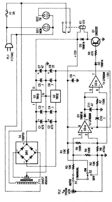
This circuit senses the video from the VCR. When the VCR is turned on, video signal is amplified by U3A and B to drive Q1, actibating K1. In this manner, it is not necessary to turn on and off two video decices every time. In many cases, this avoids the use of a cable box, the cable-ready VCR performing this function. (View)
View full Circuit Diagram | Comments | Reading(791)
SECOND_ORDER_POLYNOMIAL_GENERATOR
Published:2009/6/17 3:26:00 Author:May

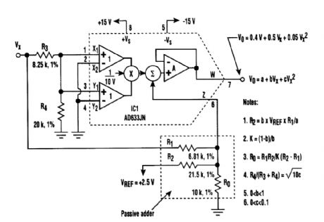
By using a circuit built with a single analog multiplier and five precision resistors, an output volt-age (Vo) can be made to create a second-order polynomial.The circuit implements the following quadratic:
VO=a+bVx+cV 2X
The input terminals of IC1 are connected to create a positive square term and present the Vx signal to the output with a 1-10-V scale factor, Incorporating the voltage-divider network (resistors R3 and R4) in the input signal path provides additional attenuation adjustment for the coefficient (c) of the square term in the quadratic. Then, the passive adder (resistors R1, R2, and RO) is wired to IC1's internal summing circuit to generate the polynomial's other two terms; the offset term (a) and the linear coefficient (b). (View)
View full Circuit Diagram | Comments | Reading(1131)
6_DIGIT_CODED_ac_POWER_SEITCH
Published:2009/6/17 3:23:00 Author:May
This seitch uses four CD4013 BE dual flip-flops, an inverter, and an optoisolator to drive a triac. The circuit can seitch 25-A ac load cuttrent. A standard 4×3 telephone keybord is used to enter a 6-digit code. In case of a wring cide, a signal is available to activate an alarm. The disarming method is a secret reset button that can be any number on the keyboard. (View)
View full Circuit Diagram | Comments | Reading(1281)
| Pages:1432/2234 At 2014211422142314241425142614271428142914301431143214331434143514361437143814391440Under 20 |
Circuit Categories
power supply circuit
Amplifier Circuit
Basic Circuit
LED and Light Circuit
Sensor Circuit
Signal Processing
Electrical Equipment Circuit
Control Circuit
Remote Control Circuit
A/D-D/A Converter Circuit
Audio Circuit
Measuring and Test Circuit
Communication Circuit
Computer-Related Circuit
555 Circuit
Automotive Circuit
Repairing Circuit