
Circuit Diagram
Index 1422
TRANSMIT_KEYER_INTERFACE_CIRCUITS
Published:2009/6/18 3:31:00 Author:May

These circuits are for use with Morse kevers and identifiers They can be used to interface various devices with the identifier circuitry (View)
View full Circuit Diagram | Comments | Reading(735)
SIMPLE_IDENTIFIER
Published:2009/6/18 3:30:00 Author:May
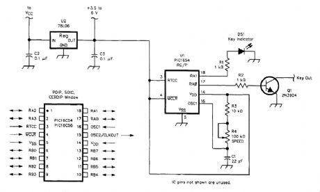
This identifier uses a PIC 16C54 microcontroller which must be programmed for your desired identifier. (View)
View full Circuit Diagram | Comments | Reading(1439)
AND_GATE
Published:2009/6/18 3:29:00 Author:May
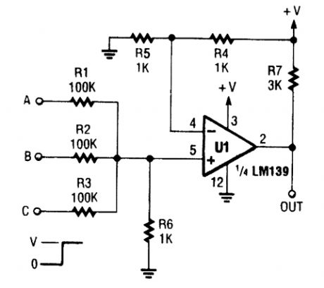
An LM1139 is configured as an AND gate(TTL or CMOS is usually used).use leftover IC sections and save an extra package in some instances. (View)
View full Circuit Diagram | Comments | Reading(0)
COMBINATORIAL_LOGIC_MULTIPLEXER
Published:2009/6/18 3:23:00 Author:May
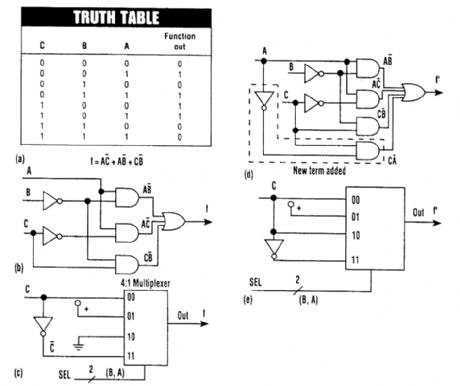
Combinatorial logic can be implemented simply by using a multiplexer instead of logic gates.Shown are the truth table(A), its logic circuit(B), and the multiplexer connections(C). If the logic circuitry is changed(D), the multiplexer would be reconnected(E). (View)
View full Circuit Diagram | Comments | Reading(996)
LONG_PERIOD_TIMER
Published:2009/6/18 3:21:00 Author:May
By using a 555 timer, time intervals of 150 minutes 60 hours can be generated with this circuit. (View)
View full Circuit Diagram | Comments | Reading(2)
2_TO_2000_MINUTE_TIMER
Published:2009/6/18 3:20:00 Author:May
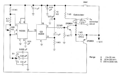
A CD4020B divider is used to divide the frequency of a 555 timer.S1 is a range selector switch that provides timing intervals of 2-20,20-200 and 200-2,000 minutes. (View)
View full Circuit Diagram | Comments | Reading(853)
LINEARIZED_RF_DETECTOR
Published:2009/6/18 3:16:00 Author:May
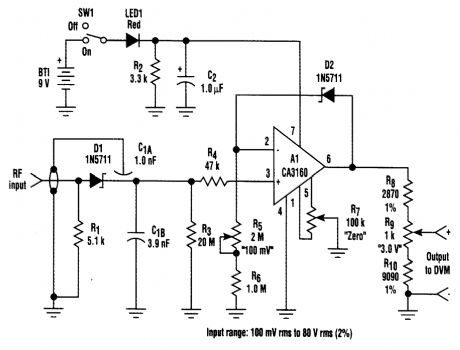
The circuit produces an extremely linear dc output for RF inputs between 80 mV rms and 4.0 mV rms. For inputs below 50 V rms, the dc output quickly drops to 0 V. (View)
View full Circuit Diagram | Comments | Reading(944)
THREE_STAGE_SEQUENTIAL_TIMER_
Published:2009/6/18 3:14:00 Author:May
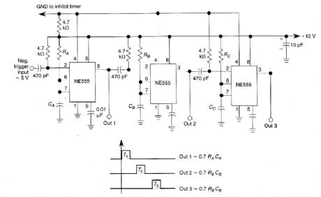
By using three 555 ICs, three sequential pulses can be generated. Output 3 can be connected back to trigger input to achieve astable operation. (View)
View full Circuit Diagram | Comments | Reading(1504)
TELE_TIMER
Published:2009/6/18 3:11:00 Author:May
The circuit is built around a 555 oscillator/ timer. The circuit provides two time periods. The long-running time period is adjustable from about 1 to 10 minutes, and the short time period is pre-set to about three seconds.
Here's how the dual timer operates. When the power is switched on, C2 begins to charge through R3, R1, Dl, and R4 to start the long-term timer period. When the voltage across C2 reaches the 555's internal switching point, the long-term timer times out, discharging C2 throughR2, D2, and pin7 ofthe 555. Duringthat time, pin 3 of the 555 is pulled to ground, acti-vating the piezo sounder.To set the short time period to about four seconds, use a 10 k resistor for R2, and for about twenty seconds use a 47 k resistor. The timing capacitor, C2, should be a good-quality, low-leakage unit. (View)
View full Circuit Diagram | Comments | Reading(981)
LOCK_DETECTOR
Published:2009/6/18 3:11:00 Author:May
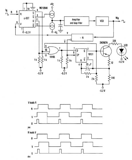
This PLL lock indicator not only can detect a 'locked or off-of-lock condition, but also even if a single pulse or transition has been missed.When being sampled by the flip-flop, if the V signal leads the input reference signal R and the rising edge of /i is lost, the D signal will remain hign throughout the interval, allowing the flip-flop to be clocked high (Fig. 26-2A). If the R signal leads the V signal when the transition is missed, the rising edge of the Tsignal will trigger the D signal of the phase detector, causing the LED to blink (Fig. 26-2B).A lock detector often is used with a phase-locked loop (PLL) or synthesizer to indicate when the loop is phase-locked with an input signal. This circuit can be helpful, but single cycle skips usu-ally frill go undetected because of the presence of the low-pass filter. (View)
View full Circuit Diagram | Comments | Reading(2305)
HIGH_SPEED_PEAK_DETECTOR_WITH_HOLD_AND_RESET_CONTROLS
Published:2009/6/18 3:08:00 Author:May
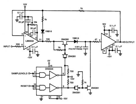
The LH0033 and LH0063 are useful in high-speed sample-and-hold or peak detector circuits be-cause of their very high speed and low-bias-current FET input stages. The high-speed peak detector circuit shown could be changed to a sample-and-hold circuit simply by removing the detector diode and reset circuitry. For best accuracy, the circuit can be trimmed with the 10-kΩ offset adjustment pot shown. The circuit has a typical acquisition time of 900 ns, to 0.1% of the final value for the 10-V input step signal, and a droop rate of 100 μV/ms, Even faster acquisition time can be achieved by re-ducing the hold capacitor value. (View)
View full Circuit Diagram | Comments | Reading(5281)
LOGIC_STATE_CHANGE_INDICATOR
Published:2009/6/18 3:07:00 Author:May

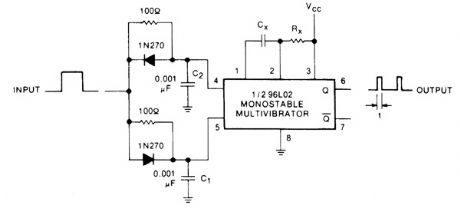


A circuit consisting of a one-shot multivibrator IC, a pair of diodes, and some resistors and capacitors delivers an output pulse when the logic state at its input terminal changes-either from high to low or from low to high. Thus, this circuit can serve as a state-change indicator or as a frequency doubler for a square-wave input.Any monostable can be used; the arrangement in the figure achieves low power dissipation(80 milliwatts)by using half of a Fairchild 96L02 transistor-transistor-logic dual multivibrator. The 96L02 is triggered when pins 3 and 5 are high and pin 4 changes state from low to high. It also triggers if pin 3 is high, pin 4 is low.The circuit shown here allows these conditions to be satisfied with a single input terminal, plus the fixed bias on pin 3; the arrangement of resistors, capacitors, and diodes automatically biases pin 5 high when transmitting a rising transition to pin 4 and biases pin 4 low when applying a falling tran-sition to pin 5.For example, if the input terminal has been low and then goes high, C1 charges through a for-ward-biased diode that shunts its 100-Ω resistor; therefore pin 5 goes high immediately. C2 charges through 100 Q; however, because its diode is back-biased, the rising level is not applied to pin 4 un-tilSis already high. Therefore, the conditions for triggering an output pulse are satisfied.The output pulse duration, f, is set by the value of time constant RXCX. (View)
View full Circuit Diagram | Comments | Reading(866)
BATTERY_PACK_AND_REVERSE_POLARITY_PROTECTION
Published:2009/6/18 3:03:00 Author:May
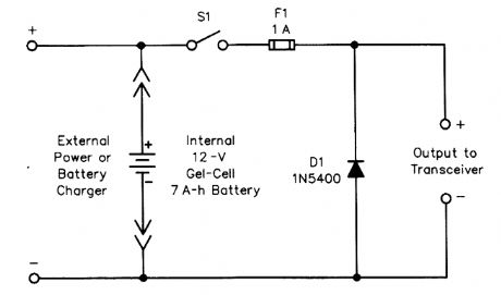
Schematic diagram and parts list for the reverse-polarity protection circuit D1 1N5400 silicon diodeF1 1-A fast-acting fuseS1 SPST rocker switch (View)
View full Circuit Diagram | Comments | Reading(2274)
PF_LINE_SAMPLER_COUPLER
Published:2009/6/18 3:02:00 Author:May
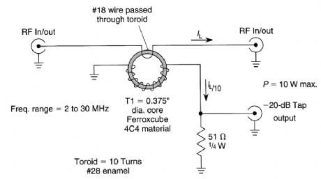
Suitable for RE line sampling, this coupler is useful where an indirect measurement of line cur-rent is needed. A 10:1 turn ratio yields a secondary current about1/10 (ideally) of the line current. A 51-Ω, resistor terminates the secondary. Insertion loss in the main line is negligible, < 0.l dB. For higher power levels, use proportionately larger core for T1. (View)
View full Circuit Diagram | Comments | Reading(738)
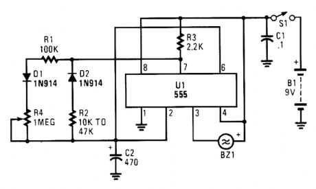
SIMPLE_TIME_DELAY_CIRCUIT
Published:2009/6/18 3:02:00 Author:May
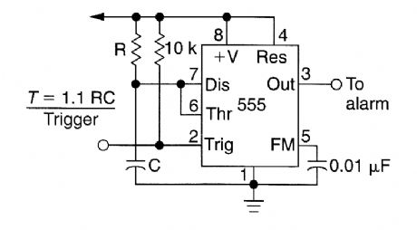
Rotating the potentiometer wiper will change the time delay from the 555 IC. (View)
View full Circuit Diagram | Comments | Reading(995)
TIME_DELAY_GENERATOR
Published:2009/6/18 3:00:00 Author:May
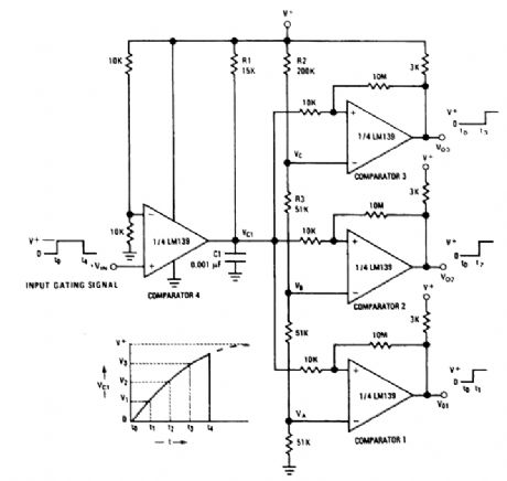
This circuit uses a charging capacitor and three comparators to read the voltage across it. (View)
View full Circuit Diagram | Comments | Reading(1592)
ELECTRONICS_NOW
Published:2009/6/18 2:59:00 Author:May


This timer circuit uses a 555IC timer and three 74LS193 counters to drive an LED display. S1 is activated by one person, who tums on piezo buzzer BZ1 via Q1 and also starts the clock; S1 is acti-vated by the other person being timed. This shuts off the timer, and the number of LEDs lit indicate, in binary form, the elapsed time. (View)
View full Circuit Diagram | Comments | Reading(2441)
CW_AUDIO_FILTER
Published:2009/6/18 2:59:00 Author:May
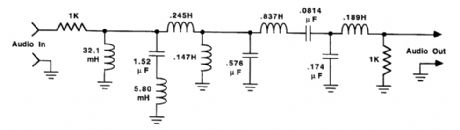
A high-performance passive filter. The center frequency is 700 Hz; -3-dB bandwidth is 200 Hz. (View)
View full Circuit Diagram | Comments | Reading(1053)
VIDEO_LINE_DECODER_II
Published:2009/6/18 2:57:00 Author:May
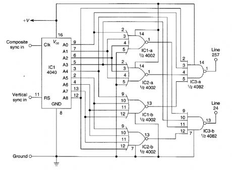
pulses useful for gating lines 24 and 257 of a video signal, but by chang-lines can be decoded. (View)
View full Circuit Diagram | Comments | Reading(700)
80_METER_SSB_RECEIVER
Published:2009/6/18 2:55:00 Author:May
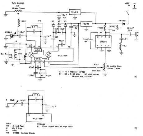
This circuit uses an MC3335P IF chip and features a 3-pole crystal filter made from microprocessor crystals. Tuning is done either with a varactor diode or air-variable capacitor, as shown.Values are for 80 meters. (View)
View full Circuit Diagram | Comments | Reading(1653)
| Pages:1422/2234 At 2014211422142314241425142614271428142914301431143214331434143514361437143814391440Under 20 |
Circuit Categories
power supply circuit
Amplifier Circuit
Basic Circuit
LED and Light Circuit
Sensor Circuit
Signal Processing
Electrical Equipment Circuit
Control Circuit
Remote Control Circuit
A/D-D/A Converter Circuit
Audio Circuit
Measuring and Test Circuit
Communication Circuit
Computer-Related Circuit
555 Circuit
Automotive Circuit
Repairing Circuit