
Circuit Diagram
Index 1402
ACCELEROMETERG_METERCIRCUIT
Published:2009/6/19 3:09:00 Author:May
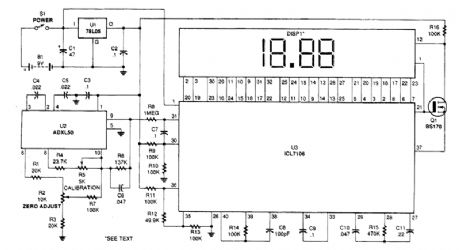
As this schematic shows,the ADXL50 accelerometer,U2,interfaces with an A/D converter,U3, to drive a 3 1/2-digit LCD module, DISPl. Because that module displays any number from -19.99 to +19.99, the circuit is designed to measure g's within that range. The heart of the circuit is U2, the ADXL50 ac-celerometer. The sensitivity of that chip is set to ±20 g's in order to accommodate the full scale capa-bility of LCD module DISP1 (19.99). Circuit gain is determined by the values of R4, R5, and R6, potentiometer R2, and R3 provides a way to manually set the zero-g voltage-output level at pin 9 of U2 to half the supply voltage-2.5V. That output voltage will vary linearly by 0.1-V/g of acceleration.In order to achieve go,od circuit performance at low g levels, the bandwidth of the amplifier is limited to about 30 Hz by C6. The digital-display section of the circuit is composed of DISP1 and U3. Included in U3 are the A/D converter, clock oscillator, storage resistors and latches, 3)6-digit seven-segment decoders, and backplane generator.The differential analog input of U3 is applied between pins 30 and 31. The positive input, pin 31, is driven by output-pin 9 of U2 through R8, a buffer resistor, and the negative input, pin 30, is biased at a fixed voltage of 2.5 V by a voltage-divider string composed of R9 and RIO.A reference voltage is required by U3. Full-scale display, 19.99, occurs when the differential, ana-log input voltage applied between pins 31 and 30 is equal to twice the reference voltage. The decimal point ofthe LCD has to be illuminated to display readings from 0.00 to 19.99. That is done by invert-ing the backplane square-wave drive signal appearing at pin 21 of U3, through MOSFET Q1, and ap-plying the 180-degree out-of-phase signal to pin 12 of DISP1. (View)
View full Circuit Diagram | Comments | Reading(4830)
FUNCTION_GENERATOR
Published:2009/6/19 3:07:00 Author:May
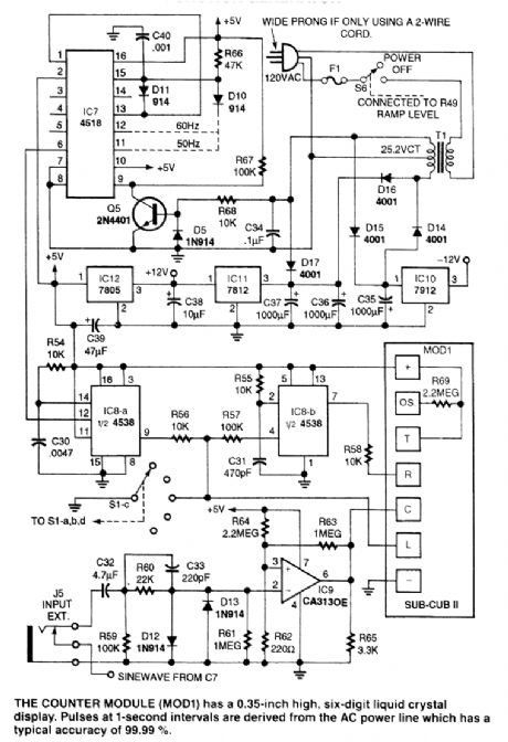
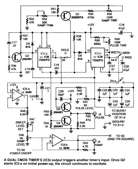
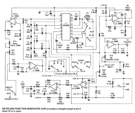
These three circuits make up an audio frequency function generator and can be individually used for custom applications. (View)
View full Circuit Diagram | Comments | Reading(0)
Linearization circuit of thermistance
Published:2011/5/6 1:21:00 Author:May | Keyword: Linearization, thermistance
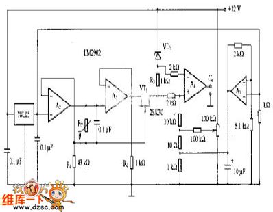
This diagram is Linearization circuit of thermistance.
In the circuit, it also is constant flow source. Its non-inverting input end is offered reference voltage by 78LO5. The output of A2 offers constant current for thermistance RT. This current is connected ground through R1. The value of constant current is determined by R1.
If RT is 5kΩ, constant current is 120μA when the voltage dropping on RT must be 0.6V. This voltage dropping adds to the source of VT1 through A3 buffer. Because the grid of VT1 is connected in one side of RT, so, grid-source voltage of VT1 is the voltage on the justified of RT. The function of R2 is flowing through idle current. The output voltage of A3 can remain unchanged when source current of VT1 changes. The justified voltage of R3 and temperature is linear relation. But R3 is in the state of floating. So, differential amplifier A4 offers this voltage. The relation between output voltage Uo and temperature changes to linear relation. (View)
View full Circuit Diagram | Comments | Reading(908)
2_TO_5_CELL_LITHIUM_BATTERY_CHARGER
Published:2009/6/19 3:06:00 Author:May
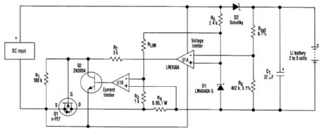
A more generally applicable circuit-design concept for recharging lithium batteries could easily accommodate different cell types and various numbers of cells. That's because both the charger out-put-voltage set point and current limit, or maximum charging current, can be adjusted by simply changing a resistor. (View)
View full Circuit Diagram | Comments | Reading(1060)
NICAD_CHARGER_ZAPPER
Published:2009/6/19 3:04:00 Author:May
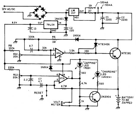
This NiCad charger/zapper has a built-in charger and zapper circuit to clear shorted NiCads. This circuit delivers a high-current pulse to trim out internal shorts. (View)
View full Circuit Diagram | Comments | Reading(1778)
FREQUENCY_TO_VOLTAGE_CONVERTER
Published:2009/6/19 3:04:00 Author:May

The AD537 can also be used to perform frequency-to-voltage conversion. The transistor pair shown here operates as an exclusive-or gate to perform the phase comparison. It locks onto the input frequency within two cycles. The configuration requires only 3 mA for frequencies up to 10 kHz. In most situations, an output buffer will be required to unload the filter. Use 0-to 5-V pulses or square waves with 40-μs minimum pulsewidth. (View)
View full Circuit Diagram | Comments | Reading(2)
RF2152 dual-mode high-power linear amplifier pin diagram
Published:2011/5/6 1:00:00 Author:May | Keyword: dual-mode, high-power, linear amplifier
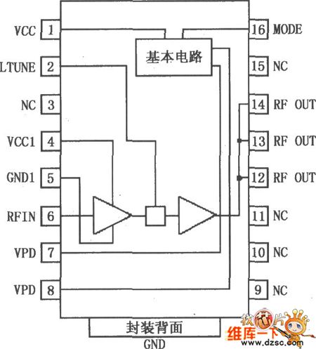
RF2152 is a high-power, high efficiency linear amplifier IC. It is used in 3V handheld systems, such as 3V CDMA/AMPS mobile cellular systems, JD-MA/TACS mobile phone and TDMA/AMPS mobile phone. RF2152 is used advanced GaAs heterojunction bipolar transistor (HBT) to treat. It is intended for dual-mode CDMA/AMPS handheld digital cellular systems devices' final linear RF enlarge, band spread system and other application with 800~950MHz working frequency. The device itself includes 50Ω input and output, so is very easy to get best power, efficiency and linear performance. RF2152 uses PSSOP-16 package, its pin array is shown in the diagram. (View)
View full Circuit Diagram | Comments | Reading(740)
INDUSTRIAL_FREQUENCY_TO_VOLTAGE_CONVERTER
Published:2009/6/19 3:02:00 Author:May

Control and process equipment often require the indication of frequency (speed or rate) of linear or rotary mechanical movement. Motion can be detected using various pulse-generating pickups and proximity detectors that output ac or dc pulsed signals.This industrial converter can serve in a wide variety of applications. The circuit operates around a quad-FET input op amp and is designed to be selfcontained or run from a bipolar supply. The in-put signal of dc pulses or ac waveforms is applied to R2.Amplifier 1, which acts as a Schmitt trigger, supplies a squarewave output of fixed amplitude to C4. Resistor R3 and capacitor C6 filter out input noise, and R4 and R5 determine the switching levels, and Zener diode 23 sets the amplitude.Amplifier 2 gives a fixed-duration pulse on the positive transition of C4, with a time constant set by C4 and R6 and the switching level set by R7 and R8. Resistor R9 and Zener diode 22 fix the am-plitude of the pulses and amplifier 3 integrates them via R10 and C5. Diode D6 blocks negative inte-gration and R11 discharges C5 with a long-time constant.Hence, the dc output of amplifier 3 is proportional to the frequency applied to the input. Amplifier 4 inverts and buffers the negative output of amplifier 3 and provides amplitude adjustment voltage.The complete circuit is linear and sufficiently accurate providing that C4 is chosen to give a pulse duration less than the maximum input frequency and that R11 > R10. (View)
View full Circuit Diagram | Comments | Reading(1075)
Charge amplifier circuit composed of the OPA128
Published:2011/6/28 3:30:00 Author:Rebekka | Keyword: Charge amplifier
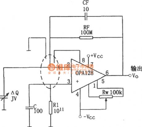
The so-called charge amplifier is amplifier circuit used to amplify the signal from the piezoelectric devices charge. The intrinsic impedance of the amplifier circuit sources is high, while the signal is very weak. The formation of the current source is only pA level. The charge amplifier need to have high input resistance and low offset current. Or when the amplifier's bias current is similar to the signal current signals, the signals might be engulfed by the current. The normal amplification will not be achieved. (View)
View full Circuit Diagram | Comments | Reading(2624)
GATE_DiP_OSCILLATOR_I
Published:2009/6/19 3:00:00 Author:May

The typical dip meter is comprised of a tuning coil,RE oscillator,a detector,and a meter as shown in A.When the meter's tuning coil is coupled to a tuned circuit resonating at the same fre-quency as the GDM,the reading dips (C).The GDM's tuning coil can be coupled to the coaxial feed line of an antenna through a few(perhaps 2 to 3)turns of wire,and used to determine the antenna's resonant frequency(D). (View)
View full Circuit Diagram | Comments | Reading(1858)
Atomizer circuit
Published:2011/5/3 3:38:00 Author:May | Keyword: Atomizer
This article describes a device which can generate mirage around miniascape's rockwork and trees, like white clouds folating in the mountains, greatly improve the ornamental value.
一、 working principle
The circuit is show in the diagram.
This article describes a device which can generate mirage around miniascape's rockwork and trees which is seemingly as if white clouds floated in the mountains, and it greatly improves the ornamental value.
一、 working principle
The circuit is shown in the diagram.
It mainly consists of ultrasonic generator, the water level controller, power supply circuit etc. Ultrasonic generator mainly consists of triode VT1, VT1 and capacitor three-point LC oscillator composed of its outside component; B is ultrasonic transducer, its natural frequency fc=1.65MHz; capacitor C1, C2 can decide oscillation amplitude, its natural frequency is a little less than fc. L1 and C2 are positive feedback elements, and their natural is a little higher than fc; VD5 is protecting diode of VT1. B is under water when pulverization. Water level controller consists of VT2, VT3, the effect is:
(1) Offer base bias current for oscillation circuit;
(2)When the water level in the miniascape is lower than set value, it can make oscillator failure of oscillation and act the function of protection. (View)
View full Circuit Diagram | Comments | Reading(3108)
BACKUP_BATTERY_MONITOR_CHARGER_ALARM
Published:2009/6/19 2:59:00 Author:May


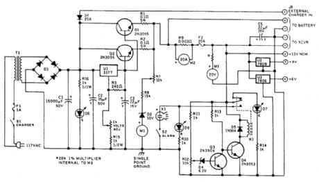
Battery Condition Meter Calibratio Lead-Acid Battery Lead Calcium RatteryColor Voltage Color VoltageRed 11.6 and below Red 11.6 and belowYellow 11.6 to 12.0 Yellow 11.6 to 12.0Green 12.0 to 13.8 Green 12.0 to 13.5Red 13.5 and higher Red 13.5 and higher
Charging voltage is constant at the normal full-charge level, so the charging current drops as full oharge is approached, and full charge is maintained with a trickle current. The charging voltage can be adjusted between approximately 10 and 15 Vdc to accommodate lead-acid (13.8 V) or lead-cal-ciurn (13.2V, 13.5V maximum) deep-cycle storage batteries.A separate connection is provided so that an extemal charger can be used when greater than 3 A is needed to charge a pa'rtially discharged battery. Intemal circuitry will maintain the charging volt-age to the battery at the nominal full-charge voltage level, regardless of the voltage supplied by the external charger, which will be 2V or more greater than that applied by the regulator to the storage battery. Warning: do not fast-charge deep-cycle storage batteries!A pair of meters calibrated to indicate 20 Vdc and 20 Adc full-scale monitor voltage and current when battery power is used.A separate, suppressed zero, expanded-scale meter calibrated over the range of about 10 to 15 Vdc allows immediate and constant indication of the state of charge of the station's backup battery.This meter scale is calibrated in bands of red, yellow, and green, as explained in the table. The nar-row yellow segment is based on the assurnption that solid-state transceivers might not operate prop-erly below +12 Vdc. The intemal power supply is used to calibrate this meter. A DMM should be used for greatest accuracy.An alarm circuit is included to indicate when the battery has been discharged by 60 percent tothe 11.6-Vdc level When battery voltage IS above 11.6 V, the green LED will be illuminated;when voltage falls to 11.6V, the green LED goes out and the red LED lights A piezo audible alarm soundsat this low voltage level unless silenced by the toggle switch controlling it.A pair offixed three-terminal regulators are included to provide+9 and+6 Vdc (View)
View full Circuit Diagram | Comments | Reading(1853)
TWO_AMPLIFIER_FLIP_FLOP
Published:2009/6/19 2:54:00 Author:May

View full Circuit Diagram | Comments | Reading(778)
TRIGGER_FLIP_FLOP
Published:2009/6/19 2:54:00 Author:May
Trigger flip flops are useful to divide an input frequency as each input pulse will cause the out-put of a trigger flip flop to'change state. Due to the absence of a clocking signal input, this is for an asynchronous logic application. A circuit that uses only one amplifier is shown. Steering of the dif-ferentiated positive input trigger is provided by diode CR2. For a low-output voltage state, CR2 shunts the trigger away from the (-) input and resistor R3 couples this positive input trigger to the (+) input terminal. This causes the output to switch high. The high-voltage output state now keeps CR2 off and the smaller value of (R5 + R6) compared with R3 causes a larger positive input trigger to be coupled to the (-) input, which causes the output to switch to the low-voltage state. (View)
View full Circuit Diagram | Comments | Reading(3)
NICAD_BATTERY_CHARGER
Published:2009/6/19 2:53:00 Author:May
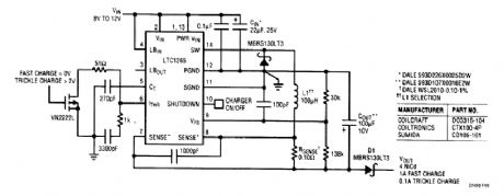
The LTC1265 is configured as a battery charger for a four-NiCad stack. It has the capability of performing a fast charge of 1A, a trickle charge of 100mA, or the charger can be shut off. In shut-off, diode D1 serves two purposes. First, it prevents the LTC1265 circuitry from drawing battery current and second, it elintinates back powering the LTC1265, which avoids a potential latch condition at powerup. (View)
View full Circuit Diagram | Comments | Reading(2089)
With a 4 wire meet method eliminating the lead resistance effects circuit diagram
Published:2011/7/1 2:12:00 Author:Rebekka | Keyword: 4 wire meet method , lead resistance effects
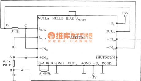
The distance measurement temperature resistance is closed to the ADT70, and its lead resistance generally can be neglected. But the leads of the platinic resistance can be up to a dozen meters and even hundreds of meters, the effects are not allow to ignore. Useing the 4 wire meet method can eliminate the influence of lead resistance. The specific circuit is shown in the figure. The characteristics of the circuit is to make the IOUTA and-INIA, IOUTB and + INIA separate from the original. It devides the line 2 into 4 connection. There are 4 nodes. Because A and C node node of the amplifier input lead has not the current, so R1, R2 lead resistance will not cause the measurement error. (View)
View full Circuit Diagram | Comments | Reading(535)
SIMPLE_TEST_AUDIO_AMPLIFIER
Published:2009/6/19 2:53:00 Author:May
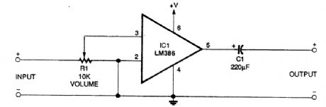
This circuit has a gain of about 20. A suitable power supply voltage is 5 to 12 V, depending on the desired audio output power level. (View)
View full Circuit Diagram | Comments | Reading(760)
LED_FLASHER
Published:2009/6/19 2:52:00 Author:May
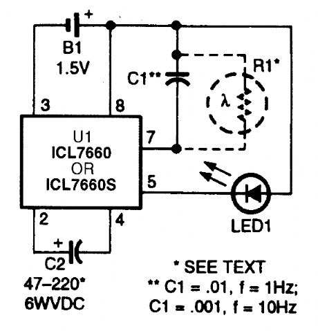
This circuit provides a low-cost way to flash an LED from a single 1.5-V source. Based on the ICL7660 dcto-dc voltage converter, the circuit makes use of an extemal capacitance (C1) on the os-cillator ratecontrol pin to decrease the charge/dump time to the desired flash rate. A dc resistance (R1) on the same pin can also be used to disable the oscillator and extend the power-cell's life. That optional dc resistance (in the form of a photoconductive cell) will shut off the oscillator in daylight. (View)
View full Circuit Diagram | Comments | Reading(3628)
THREE_CELL_LITHIUM_CHARGER
Published:2009/6/19 2:52:00 Author:May
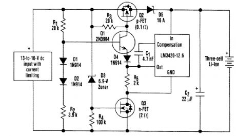
This 3-A, three-cell charging circuit for lithium batteries includes a built-in on/off switch made up of Q3, R4, and D3. When a dc input is present, D3 turns on Q3, which allows current to flow through the LM3411 and Q1. If dc voltage is removed, Q3 turns off, cutting battery drain to zero. (View)
View full Circuit Diagram | Comments | Reading(1059)
DIGITAL_THREE_PHASE_WAVE_GENERATOR
Published:2009/6/19 2:51:00 Author:May
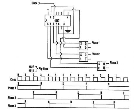
With a simple digital circuit, three-phase square waves can be produced from a single-phase square-wave signal source. The timing diagram shows that the second and third phases are 1200 and 2400 behind the first phase, respectively.The frequency range over which the three-phase outputs will occur is limited only by the capa-bility of the logic used. The output frequency is 1/6 of the input frequency. (View)
View full Circuit Diagram | Comments | Reading(911)
| Pages:1402/2234 At 2014011402140314041405140614071408140914101411141214131414141514161417141814191420Under 20 |
Circuit Categories
power supply circuit
Amplifier Circuit
Basic Circuit
LED and Light Circuit
Sensor Circuit
Signal Processing
Electrical Equipment Circuit
Control Circuit
Remote Control Circuit
A/D-D/A Converter Circuit
Audio Circuit
Measuring and Test Circuit
Communication Circuit
Computer-Related Circuit
555 Circuit
Automotive Circuit
Repairing Circuit