
Circuit Diagram
Index 1414
ANTENNA_TUNER
Published:2009/6/18 23:18:00 Author:May
This is a circuit diagram of the Collins Model 1805-1 antenna tuner. Three unbalanced configurations are available, two of which form an L-network and the other is a π-network. The tuning range is impressive. (View)
View full Circuit Diagram | Comments | Reading(124)
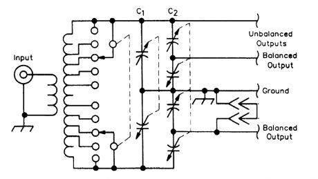
MATCHBOX_ANTENNA_TUNER
Published:2009/6/18 23:17:00 Author:May

C1 is a split stator capacitor and C2 is a dual differentiaJ capacitor. The top unbalanced output connection is used for high-impedance unbalanced loads, and the other is used for low-impedance unbalanced loads. In the latter case, the unused balanced load connection is grounded. (View)
View full Circuit Diagram | Comments | Reading(1126)
TUNABLE_FM_ANTENNA_BOOSTER
Published:2009/6/18 23:16:00 Author:May

This two-transistor amplifier circutt with tunable Lank circuits boosts Lhe distant FM signals Coils L1 and L2 are 1 1/2 turns#20 AWG bail tinned wtre wound around a 2/3 diameter mandrel. (View)
View full Circuit Diagram | Comments | Reading(3397)
SIREN
Published:2009/6/18 23:12:00 Author:May
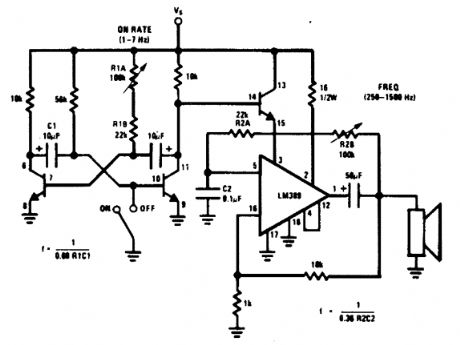
An LM380 audio IC is configured as a feed-transistor astable modu-a low frequency, which back audio oscillator. A lates this oscillator at a low frequency, which produces a siren tone. (View)
View full Circuit Diagram | Comments | Reading(2)
INDUCTANCE_WITH_DVM_MEASURING_CIRCUIT
Published:2009/6/18 23:10:00 Author:May
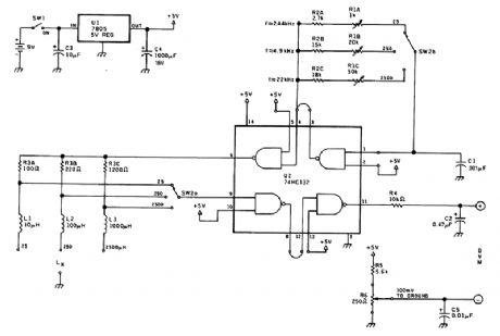
The inductance meter comprises an oscillator and pulse shaper. The square wave from the oscillator is differentiated and the differentiator output is shaped and read on a DVM. This will be proportional to inductance. R1A, B, C set calibration and R6 is an offset control. (View)
View full Circuit Diagram | Comments | Reading(1893)
SOUND_EFFECTS_GENERATOR
Published:2009/6/18 23:10:00 Author:May
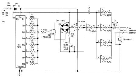
The circuit consists of four parts: a binary counter, a D/A converter, a VCO, and an audio output amplifier. The speed at which the counter counts depends on the frequency of the output of the VCO, which in turn is determined by the output of the counter. That feedback loop gives this circuit its characteristic output.The initial frequency of oscillation is determined by potentiometer R11. The VCO first oscillates at a relatively low frequency, and it gradually picks up speed as the control voltage supplied by the D/A converter increases.The D/A converter is simply the group of resistors RI through R8. When none of IC1's outputs is ac-tive, little current will flow into the base of Q1, so the VCO's control voltage will be low. As more and more counter outputs become active, base current increases, and so does the VCO's frequency of oscillation.The VCO itself is composed of IC2-a, IC2-b, and Q1; the timing network is D1 through D4, C1, R10, and R11. The diode bridge functions basically as a voltage-controlled resistor. The buffer amplifier is made up of the four remaining gates from IC2, all wired in parallel. The volume is sufficient for experimental purnoses, but you might want to add an amplifier, speaker, or both. (View)
View full Circuit Diagram | Comments | Reading(2344)
FM_AUTO_RADIO_DIVERSITY_ANTENNA
Published:2009/6/18 23:08:00 Author:May


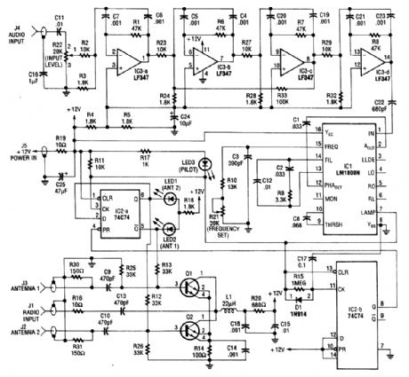
A second antenna, installed on your vehicle as far away from the original equipment antenna as practical, provides the second FM signal. The figure is a simplified block diagram of the diversity system.The cables from both antennas are connected to the electronic antenna switch. The 19-kHz pi-lot signal from the receiver's audio output is passed through a high-gain bandpass active filter, which attenuates audio programming that is much stronger than the pilot signal. After amplification, the pi-lot subcarrier becomes the reference frequency for a phase-locked loop (PLL) circuit. The output of the PLL locks to the 19-kHz pilot signal and functions as a subcarrier detector. When the reference frequency becomes noisy, the PLL will lose lock and trigger the flip-flop, whose output switches the state of the electronic antenna switch,This action switches the alternate antenna into the system while disabling the original antenna.
If that second antenna is positioned for better reception,the received signal will clear,and the PLL will again lock to the subacrrier and hold the switch in that state until the pilot signal drops out again,If the second antenna does not restore the pilot signal reception after a0.1-second delay,the primary antenna is switched back on.When the radio is receiving AM, the absence of the 19- kHz subcarrier will also reactivate the primary antenna that is tuned to the receiver tor the best AM reception. (View)
View full Circuit Diagram | Comments | Reading(1723)
Little Modifying Tianpeng AP-321 Power Amplifier Circuit
Published:2011/7/28 17:45:00 Author:Robert | Keyword: Modifying, Tianpeng, Power Amplifier
Openning its case, the resistances are all five-ring metal films, dozens of red CBB small capacitors are high-quality. And the key places even use the sanyo 105℃ electrolytic capacitor. The coupling capacitors are two ELNA no-polarity series normal products. The audio source switch uses the long-axis switch. The kara OK chip uses the Japanese Mitsubishi company's M50195P. The large-power output tube is Toshiba company's 2SC3280 and 2SA1301. When modifying the machine later it alse find that all triodes and resistances have been strictly paired. The back board has two groups of output ports which could connect to a couple of speakers at the same time. It can uses the a switch on front board for AB contrast audition. The Kara OK and the tone stage all have the switchs. When they are not used they could be closed to avoid the bad effects on the sound quality, which is very practical. (View)
View full Circuit Diagram | Comments | Reading(2807)
LOW_LEVEL_SOUNDER
Published:2009/6/18 23:07:00 Author:May
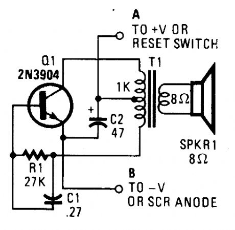
This is a simple low-level noise maker that's ideally suited to certain alarm applications. When the sounder is Iocated in another part of the building, the sound level is loud enough to be heard, but is not loud enough to wam off an intruder. A single 2N3904 npntransistor is connected in a Hartley audio oscillator, with a 1 kΩ to 8-Ω tran-sistor-output transformer doing double duty.The circuit produces a single-frequency tone that can be varied in frequency by changing the value of either or both R1 and C1. Increasing the value of either component will Iower the output frequency and decreasing their values will raise the frequency. Don't go below 4.7 kΩ for R1 because you could easily destroy Q1. (View)
View full Circuit Diagram | Comments | Reading(803)
Photoelectric automatic controller circuit diagram
Published:2011/6/23 22:26:00 Author:Rebekka | Keyword: Photoelectric automatic controller
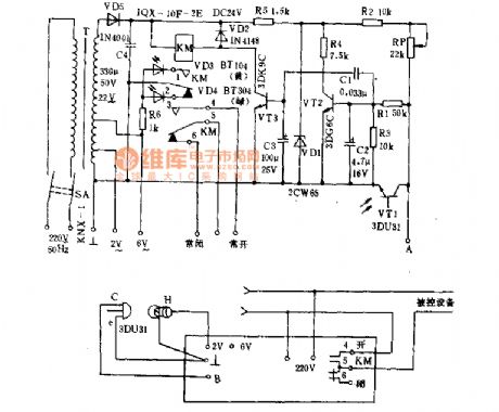
Photoelectric automatic controller is - kind of fast action of light control devices. It is used for the automatic start, automatic stop hunger, moving the door to protect from power counting, automatic alarm, etc. It is suitable for mechanical instruments, metallurgy, textile, paper and other production processes. Its working principle is shown as below. 220V AC passes T Buck and secondary turns into 22V. A stable voltage provided for VT2 regulated by the VD5, C4 rectifier, VDl. When the VT1 element photodiode is exposed to light, it passes the resistance and make the vT2 base key rise. The VT2 turns into saturation mode. (View)
View full Circuit Diagram | Comments | Reading(566)
MINIATURE_BROADBAND_ANTENNA_3_TO_30_MHz
Published:2009/6/18 23:06:00 Author:May
A short dipole antenna and impedance converter combined together can be rotated to null out an interfering signal. The converter supplies a tremendous current gain so that the voltage appear-ing at the dipole's output eventually drives a 75-Ω load. (View)
View full Circuit Diagram | Comments | Reading(1254)
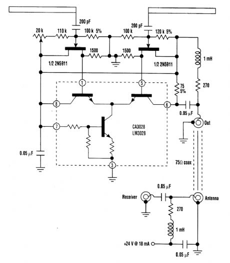
REMOTE_TUNED_ACTIVE_HF_ANTENNA
Published:2009/6/18 23:04:00 Author:May
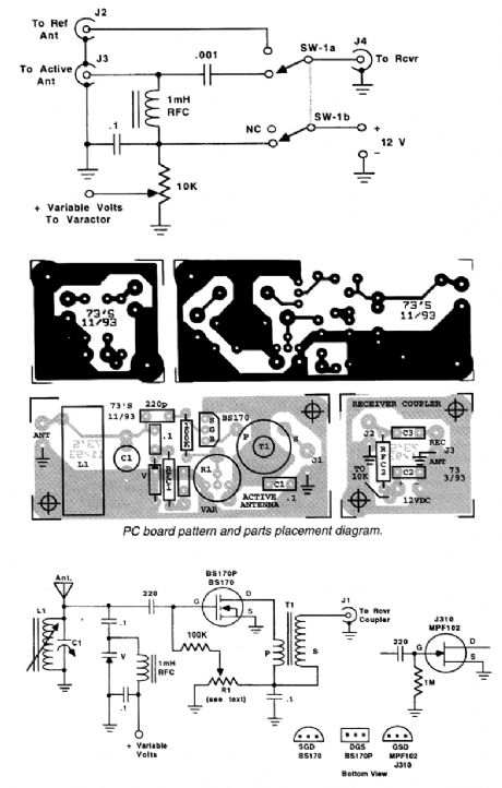
An MV1662/S varactor diode tunes this active antenna/preamplifier.R1 varies gate bias on the BS170 FET. T1 is a 3:1 toroidal winding suitable for the frequencies of interest. (View)
View full Circuit Diagram | Comments | Reading(2823)
SINGLE_CHIP_DIGITAL_VOLTMETER
Published:2009/6/18 23:04:00 Author:May
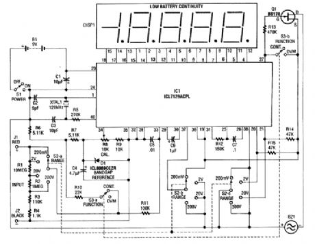
This 4 1/2-digit DVM circuit is built around a Maxim ICL7129ACPL A/D converter and LCD driver. An ICL8069 CCZR 1.2-V band-gap reference diode is used for a voltage reference. S2a-b-c select one of four ranges up to 200 V (maximum). The meter also has a piezoelectric buzzer for continuity testing. S3 selects either DVM or continuity. Crystal 1 can be changed to 100 kHz if maximum rejection of 50 Hz is desired. The crystal normally provides 120 kHz for best 60-Hz rejection. This is caused by the dual-slope conversion technique used in IC1. (View)
View full Circuit Diagram | Comments | Reading(1580)
DUAL_TONE_SOUNDER
Published:2009/6/18 23:04:00 Author:May
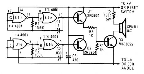
An outside horn-type speaker works best with the circuit. However, such devices require a great deal of power, so this sounder should only be used in alarm circuits where at least a 6-A SCR is used as the sounder driver.A single CMOS 4001 quad 2-input NOR gate, two 2N3904 general-purpose npn transistors, and a single MJE3055 power transistor combine to generate a two-tone output. Gates UI-a and UI-b are configured as a simple feedback oscillator with R2 and C2 setting the oscillator's frequency. With the values shown, the circuit oscillates at about 500 Hz.Gates U1-c and U1-d are connected in a similar oscillator circuit, but they operate at a much lower frequency. The oscillator frequencies (and thus the tones that they produce) can be altered by increasing or decreasing the values of R1 and C1 for the low-frequency oscillator and R2 and C2 for the high-frequency oscillator. Decreasing the values of those components will increase the frequency; increasing their values will decrease the frequency.The two oscillator outputs are connected to separate amplifiers (configured as emitter follow-ers), whose outputs are used to drive a single power transistor (Q3, an MJE3055). A 10-Ω, 5-W re-sistor, R5, is used to limit the current through the speaker and Q3 to a safe level. To boost the sound level, R5 can be replaced with another speaker. (View)
View full Circuit Diagram | Comments | Reading(1084)
ALARM_TONE_GENERATOR
Published:2009/6/18 23:00:00 Author:May
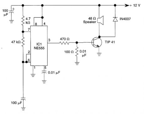
In this alarm tone generator, a TIP41 transistor is used as a speaker driver. R1, R2, and C1 determines the frequency which is 1400 Hz with the values shown. (View)
View full Circuit Diagram | Comments | Reading(2226)
ELECTRONIC_GONG
Published:2009/6/18 22:59:00 Author:May
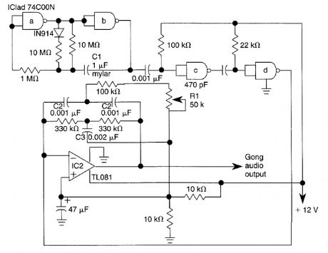
The electronic gong is comprised of an oscillator (built around half of a 74COON quad 2-input NAND gate), an active twin-T filter (built around a TL081), and will drive an audio amplifier IC such as an LM386N. Pulses from astable multivibrator IC1 cause the twin-tee active filter U2 to ring, producing a damped sinusoidal output. C1 varies rate and C2-C3 vary gong frequency. Adjust RI for best tone sound. (View)
View full Circuit Diagram | Comments | Reading(3419)
A_D_CONVERTER_FOR_PCs
Published:2009/6/18 22:57:00 Author:May
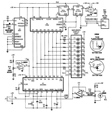
An ADC0804 A/D converter converts analog data to digital. This is fed ister and converted to serial data. U3 provides a baud-rate clock. U4A and start and stop bits needed at beginning and end of each data word. (View)
View full Circuit Diagram | Comments | Reading(3459)
SPACE_AGE_SOUND_MACHINE
Published:2009/6/18 22:55:00 Author:May
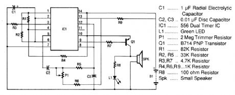
The space-age sound device uses a 556 dual-times IC to produce a phasor sound. That IC is ac-tually two 555 timer ICs in one 14-pin package, as shown in the schematic. Each timer inside the 556 is connected in an astable multivibrator mode.The first timer has its frequency set by R1, R2, and C1. Its output appears on pin 5 and it is cou-pled through C2 and R5 into the trigger input of the second timer. The second timer has an ad-justable frequency that is controlled by P1, R6, and C3.In the second timer, the first frequency mixes with the second frequency and produces the pha-sor-like sounds. The output of the second timer, which has the two signals mixed together, is brought from pin 9 through limiting resistor R7 to the input of Q1. The function of pnp gerrnanium power transistor Q1 is to amplify the signal to the level that is needed to drive the speaker. The green LED, L1, converts electrons directly into visible photons (light) in time with the pulses from the speaker. The purpose of resistor R8 is to limit the current through the LED to a safe level. (View)
View full Circuit Diagram | Comments | Reading(2473)
HIGH_SPEED_A_D_CONVERTER_SYSTEM
Published:2009/6/18 22:54:00 Author:May
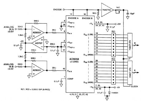
The AD8001 is well suited for driving high-speed analog-to-digital converters, such as the AD9058.The AD9058 is a dual 8-bit 50 Msps ADC. In the circuit shown, there are two AD8001s driving the in-puts of the AD905f8 which are configured for 0- to +2-V ranges. Bipolar input signals are buffered, amplified (-2x), and offset (by +1.0 V) into the proper input range of the ADC. Using the AD9058's internal +2-V reference connected to both ADCs (as shown) reduces the number of external com-ponents required to create a complete data acquisition system. The 20-Ω resistors in series with ADC input are used to help the AD8001 drive the 10-pf' ADO input capacitance. The two AD8001s only add 100 mW to the power consumption while not limiting the performance of the circuit. (View)
View full Circuit Diagram | Comments | Reading(1020)
POPULAR_ELECTRONICS
Published:2009/6/18 22:53:00 Author:May
The electronic level uses a pa:r ofphototransistors and an infrared LED to sense bubble position In this circuit,the amounts of infrared radiation received by phototransistors Q1 and Q2 are translated by op-amp U1 and dual-timer U2 into either a steady tone,or a fast-or slow-pulsing one. (View)
View full Circuit Diagram | Comments | Reading(0)
| Pages:1414/2234 At 2014011402140314041405140614071408140914101411141214131414141514161417141814191420Under 20 |
Circuit Categories
power supply circuit
Amplifier Circuit
Basic Circuit
LED and Light Circuit
Sensor Circuit
Signal Processing
Electrical Equipment Circuit
Control Circuit
Remote Control Circuit
A/D-D/A Converter Circuit
Audio Circuit
Measuring and Test Circuit
Communication Circuit
Computer-Related Circuit
555 Circuit
Automotive Circuit
Repairing Circuit