
Circuit Diagram
Index 1906
Night linear measuring benchmarking circuit
Published:2011/5/9 3:50:00 Author:Christina | Keyword: Night, linear measuring pole
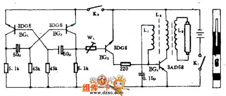
This benchmarking's night visual range is not less than 500m, with four 2-type batteries, this device can continuously works more than 30 hours, and it can be used in the night linear measurement applications or used as the signal marking equipment.
The interval oscillator is composed of the BG4 and L, this interval oscillator changes the 6V DC current into the 200V AC current and turns on the 3W cold cathode fluorescent tube as the night vision benchmarking's light source. The lamp tube can use three colors: red, white and green. BG3 is the switch tube, it is controlled by the oscillator to make the lamp tube produces flash. K2 is the work changing switch, if you need the lamp tube always turns on, you should cut off it.
(View)
View full Circuit Diagram | Comments | Reading(579)
Electrical bridge circuit
Published:2011/5/10 8:32:00 Author:Christina | Keyword: Electrical bridge
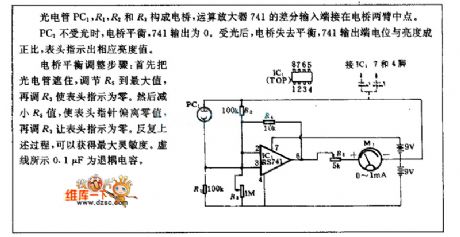
The Electrical bridge circuit is as shown:
The E-bridge is composed of the phototube PC1, R1, R2 and R3, the operational amplifier 741's differential input port connects to the middle-point of the E-bridge's two arms.
When the PC1 has no light, the e-bridge is balance, the output of 741 is 0. When the PC1 has light, the e-bridge is out of balance, the electric potential of 741 output port is proportional to the brightness, the header indicates the corresponding brightness value.
The bridge balance adjustment step: first you need to cover the photocell, then adjust R5 to the maximum value, and adjust R3 to make the meter indicates to zero. Then decrease the value of R5 to make the pointer deviation from zero, and adjust R3 to make the meter indicates to zero. Repeat this process and you can get the maximum sensitivity. The dotted line showns the 0.1uF decoupling capacitor. (View)
View full Circuit Diagram | Comments | Reading(697)
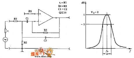
The Band-pass filter circuit which is composed of the amplifier
Published:2011/5/10 22:40:00 Author:Christina | Keyword: Band-pass filter, amplifier
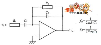
The Band-pass filter circuit which is composed of the amplifier is as shown:
(View)
View full Circuit Diagram | Comments | Reading(575)
SCR stepless light-adjustment and speed-adjustment (two-way) circuit
Published:2011/5/10 22:33:00 Author:Christina | Keyword: SCR, stepless, light-adjustment, speed-adjustment, two-way
View full Circuit Diagram | Comments | Reading(899)
Op-amp device logarithmic tables circuit
Published:2011/5/10 22:30:00 Author:Christina | Keyword: Op-amp, logarithmic tables
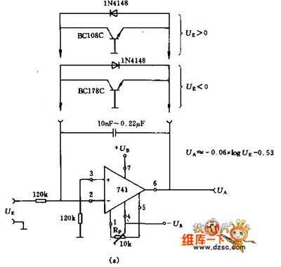
The op-amp device logarithmic tables circuit is as shown:
Figure (a) circuit: you can choose the NPN or PNP transistor according to the input signal's polarity, the voltage can be adjusted by the adjusting potentiometer RP.
Figure (b) circuit can be used as the anti-tachometer, also you can choose the NPN or PNP transistor according to the input signal's polarity. (View)
View full Circuit Diagram | Comments | Reading(1413)
Litleswan XQB50-801 washing machine principle circuit
Published:2011/5/9 3:49:00 Author:Christina | Keyword: Litleswan, washing machine, principle circuit
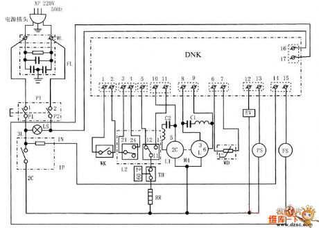
The Litleswan XQB50-801 washing machine principle circuit is as shown:
(View)
View full Circuit Diagram | Comments | Reading(1081)
Single-chip TRMS Power Measurement System AD8362 Demodulation Circuit
Published:2011/5/9 22:52:00 Author:Sharon | Keyword: Single-chip, TRMS, Power Measurement System, Demodulation
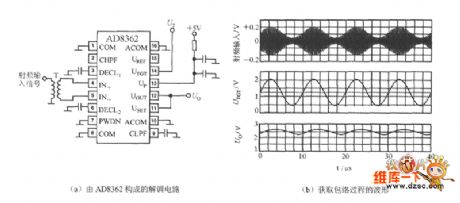
AD8362's UTGT side can constitute demodulation circuit. Take the envelope from the RF amplitude and restore it to the low and middle frequency signal before demodulation. The waveforms of the applied demodulation circuit and the process of obtaining envelope are shown in Figure (a), (b) below. It is assumed that the input signal is modulated 100kHz sine wave, and the carrier frequency is 100MHz. Link a voltage UT with an average of 1.25V, and 0.75V peak into the 14 feet, then the 12 feet's output voltage Uo is the 100kHz sine wave signal after its demodulation.
(View)
View full Circuit Diagram | Comments | Reading(1415)
The Main Technology Parameter Circuit of Mazda Ignition System
Published:2011/5/11 0:49:00 Author:Borg | Keyword: Igniting Technology, Parameter
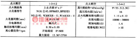
(5) the main specifications of the ignition system(as shown in figure 4)
(View)
View full Circuit Diagram | Comments | Reading(659)
The Encoding Intergrated Circuit of the BT864 Digital Video
Published:2011/5/10 22:06:00 Author:Borg | Keyword: Encoding Intergrated Circuit, Digital Video
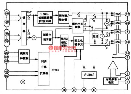

BT864 is a intergrated circuit of digital video encoding specially designed for video systems, which is widely used in many kinds of VCD and DVD players.
1.Function Features
The BT864 intergrated circuits support NTSC-M(China, Japan),PLB、D、G、H、I(Europe, Asia),PLA-M、PAL-N、PAL-NC. It has sub-circuits of the latche, brightness processing unit,color processing unit, CCTV subtitle processing unit,teletext unit,DAC and 12C interface,etc, whose internal circuit if chips are shown in Figure 1.
Figure 1 the internal circuit of BT864 chips
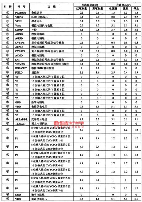
2.pin functions and relevent data
BT864 intergrated circuits are pinned with 52 pinnings, whose pin functions and data are listed in Table 1.
Table 1. pin functions and relevent data of the BT864 intergrated circuit (View)
View full Circuit Diagram | Comments | Reading(666)
W723 High-Voltage Current-Limiting Protection Circuit
Published:2011/5/7 6:03:00 Author:Robert | Keyword: High-Voltage, Current-Limiting, Protection


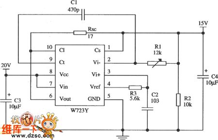
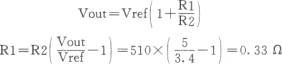
The application circuit shown in the picture below with output voltage higher thanreferenced voltage is composed of the W723 multi-port adjustable positive stabilizer. There is current limiting protectionin this circuit and the output voltage is adjustable from 7V to 36V. The input voltage in the picture is 20V, and its output voltage is 15V. The circuit in the picture also changes the output voltage by changing the sample resistance's voltage partial pressure ratio. The R2's caculation method is shown below. In its formula Vref is the referenced voltage of the stabilizer which is about 7.2V; the current-limiting resistance R3's caculation is shown below which can be taken 17Ω.
(View)
View full Circuit Diagram | Comments | Reading(1505)
Current Limiting Protection Application Cirrcuit Composed of WB705
Published:2011/5/8 6:43:00 Author:Robert | Keyword: Current Limiting, Protection, Application

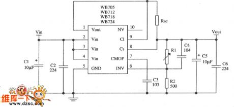
The picture shown below is about the current-limiting protection application cirrcuit with output voltage of 5V and output current of 1.5A which is composed of WB718 multi-port adjustable positive integrated stabilizer. The input voltage of the circuit can be maximum 16.8V and minimum 12.1V. The C1 and C2 are filter capacitors whose value can be choosed based on the current value. The more load current is, the more the capacitor value is required, which would reduce the ripple value of the stabilizer input port. C3 is a compensation capacitor used to prevent the oscillation effects. If the circuit has no oscillation, C3's value can be considerable less. Because C3 is connected directly to the stabilizer internal amplifier through its 7 foot. If its value is too big, that will influence the magnification. C4 can make the variation value of output voltage ΔVout to couple directly to the 6 foot of the stabilizer internal sampling port which can improve ripple rejection ratio. C5 and C6 is the capacitor to output filter wave. R1 and R2 is sampling resistance and they suit for the formula shown below. In its formula, Vref is the stabilizer's base referenced voltage with value of 3.4V. Because Vref has some extent discrete features, it should be a little bigger than the caculation result of R1 when it's chosen to use.
(View)
View full Circuit Diagram | Comments | Reading(650)
High reliable programmable integrated temperature controller TMP01 circuit diagram
Published:2011/5/10 22:12:00 Author:Nicole | Keyword: temperature controller
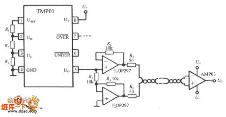
The temperature singal which is exported form TMP01 5-foot is a analog voltage, it will introduce outside interference easily when in industrial site. So it can adopt twisted-pair transmission singal, the circuit is as shown. Firstly, it uses a OP297 to divided U0 into two parts singals, then the singal is transported by twisted-pair, at last, it uses a AMP03 to receive and restore singal in the terminal. Besides amplifying the temperature singal, the differential amplifier which is composed of AMP03 also can reduce the twisted-pair's noise voltage 95dB, after it is restored, it can obtain undistorted signal voltage U0.
(View)
View full Circuit Diagram | Comments | Reading(797)
Practical band-pass filter principle circuit diagram
Published:2011/5/10 22:19:00 Author:Nicole | Keyword: band-pass filter
In negative feedback branch, this circuit is a bandstop filter, then it only allow the frequency singal which is blocked down by feedback branch to pass.
(View)
View full Circuit Diagram | Comments | Reading(731)
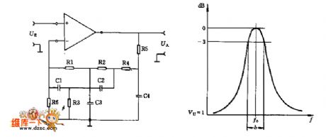
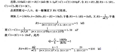
Usual band-pass filter circuit diagram
Published:2011/5/10 22:25:00 Author:Nicole | Keyword: band-pass filter
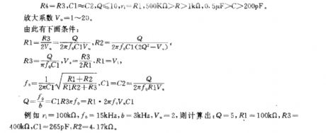
In this circuit, the R1 value is decided beforehand, the value is similar to the singal source internal resistance r. The principle of parameters selection is:
(View)
View full Circuit Diagram | Comments | Reading(679)
Thermocouple amplifier (ISO122P/124, INA101) circuit diagram
Published:2011/5/10 21:45:00 Author:Ecco | Keyword: Thermocouple , amplifier
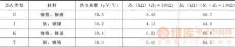
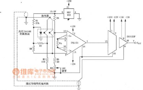
The thermocouple amplifier circuit composed of ISO122P/I24 and INA101 instrumentation amplifier, REF102 voltage reference is shown as the chart, it has the features of loop elimination, cold junction compensation and the high scale turning off end. Thermocouple can test temperature in the field, the temperature signal is converted to voltage signal and amplified by instrumentation amplifier INA101 and sent to ISO122P/124, and it is isolated amplified output by the ISO122P/124. The resistor RG is used to set the INA101 gain. The circuit is characterized by a thermocouple connecting to the ground of ISO122P/124 secondary side, that is the formation of the same potential, thereby it eliminates the interference caused by ground loops. Diode 1N4148 is the cold junction compensation of the thermocouple, 1MΩ resistor constitutes the high-end off circuit. The type and parameters of ISA are listed in the table below.
(View)
View full Circuit Diagram | Comments | Reading(2540)
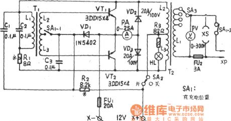
TJ-200VA emergency power supply circuit diagram
Published:2011/5/10 21:50:00 Author:Ecco | Keyword: emergency , power supply
TJ-200VA emergency power supply circuit diagramis shown as the chart.
(View)
View full Circuit Diagram | Comments | Reading(570)
LED flashing circuit diagram
Published:2011/5/10 21:47:00 Author:Ecco | Keyword: LED flashing
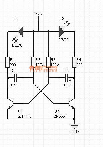
LED flashing circuit diagram is shown as the chart.
(View)
View full Circuit Diagram | Comments | Reading(1252)
ZD12 150VA emergency power supply circuit diagram
Published:2011/5/10 21:49:00 Author:Ecco | Keyword: 150VA , emergency , power supply
ZD12 150VA emergency power supply circuit diagramis shown as the chart.
(View)
View full Circuit Diagram | Comments | Reading(554)
Unipolar reversed circuit diagram composed of ISO100
Published:2011/5/10 21:29:00 Author:Ecco | Keyword: Unipolar , reversed
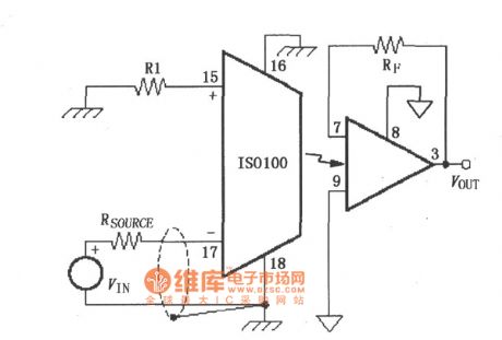
Unipolar reversed circuit diagram composed of ISO100 is shown as the chart. The circuit is a reversed amplifier, which can enlarge the unipolar input signal VIN, it requires VIN ≥ 10μA × Rsource to ensure the normal work of internal LED, photodiode, of which Rsource is internal resistor of the signal source. Inverting amplifier gain is decided by the RF, R1, that is, VOUT =- VIN (RF/R1).
(View)
View full Circuit Diagram | Comments | Reading(522)
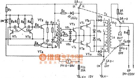
SD-120A dual-function emergency power supply circuit diagram
Published:2011/5/10 21:13:00 Author:Ecco | Keyword: dual-function , emergency power supply
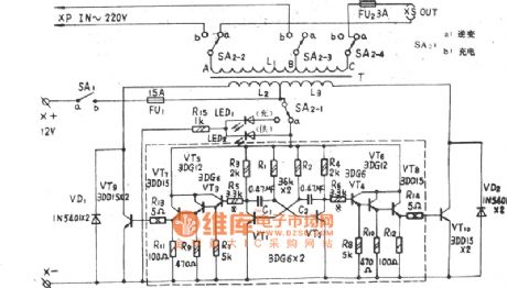
SD-120A dual-function emergency power supply circuit diagram is shown as the chart.
(View)
View full Circuit Diagram | Comments | Reading(743)
| Pages:1906/2234 At 2019011902190319041905190619071908190919101911191219131914191519161917191819191920Under 20 |
Circuit Categories
power supply circuit
Amplifier Circuit
Basic Circuit
LED and Light Circuit
Sensor Circuit
Signal Processing
Electrical Equipment Circuit
Control Circuit
Remote Control Circuit
A/D-D/A Converter Circuit
Audio Circuit
Measuring and Test Circuit
Communication Circuit
Computer-Related Circuit
555 Circuit
Automotive Circuit
Repairing Circuit