
Circuit Diagram
Index 1907
Unipolar mode noise reducing method circuit diagram composed of ISO100
Published:2011/5/10 20:46:00 Author:Ecco | Keyword: Unipolar mode , noise reducing method
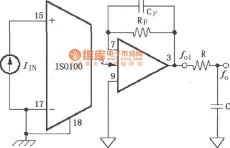
Unipolar mode noise reducing method circuit diagram composed of ISO100 is shown as the chart. In the unipolar mode, the noise is produced primarily by the conductive hole of optical components. If it does not need to work in the whole frequency range of 60kHz, the feedback loop can be added a capacitor CF to limit the output noise, and it would get a better effect while adding a RC low-pass filter.
(View)
View full Circuit Diagram | Comments | Reading(662)
The Fog Lamp,Width Lamp and Instrument Lamp Circuit of Volga 3102
Published:2011/5/10 8:48:00 Author:Borg | Keyword: Fog Lamp, Width Lamp, Instrument Lamp
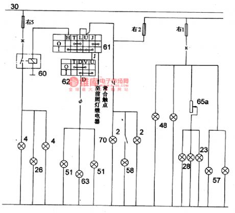
As shown in figure 5 is the fog lamp,width lamp and instrument lamp circuit of Volga 3102
2-left(front,rear)width; 4-front(left,right)width; 23-speedmeter indicator; 26-fog lamp indicator; 28-instrument indicator; 48-right(front,rear)width lamp; 51-rear(left,right) fog lamp; 57-license plate lamp;58-trunk lamp; 60-fog lamp relay; 61-fog lamp switch; 62-rear fog lamp switch; 63-rear fog lamp indicator (View)
View full Circuit Diagram | Comments | Reading(523)
Temperature protection circuit working in the AC grid
Published:2011/5/9 20:31:00 Author:TaoXi | Keyword: Temperature protection, AC grid
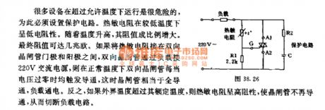
It is very dangerous that many devices are working with the over-allowable temperature, so we must set the protection circuit. The thermistor showes the low resistive in lower temperature. With the increasing of temperature, it's resistance increases in proportion. The final resistance can be up to several megohms. If we add the thermistor between the two-way SCR's cathode and anode to let the two-way SCR connects to the 220 AC power supply through the load, so in the normal temperature, the two-way SCR will be trig whenever the voltage is over-zero, at this time, the SCR is equivalent to the entire conduction, and the load gets the power. Otherwise, if the outside temperature exceeds the rated temperature, the thermistor will be high resistive, the so that the thyristor is not conduction any more to cut off the load circuit. (View)
View full Circuit Diagram | Comments | Reading(843)
Sitting Position Reminder(2)
Published:2011/5/10 0:37:00 Author:Sue | Keyword: Sitting Position, Reminder
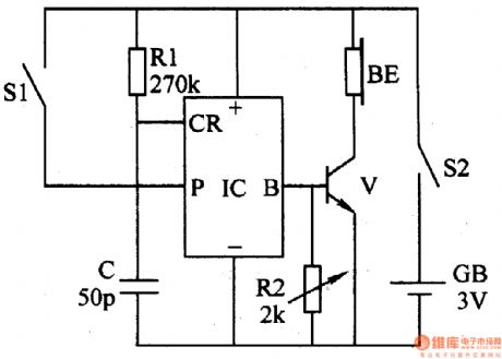
The reminder introduced here will be put on the user's ears or hat. When the user's sitting position is not proper, it can make the warning sound of Please pay attention to your sitting position . It can be used to help office stuff and students to keep proper sitting position and avoid myopia, or to be used as doze reminder for drivers.
Working principle:
As seen in the figure 6-213, the reminder consists of mercurial switch(as leaning angle sensor)S1, resistor R1,R2, capacitor C, audio integrated circuit IC, transistor V, earphones BE, power switch S2 and battery GB.
When the sitting position is proper, S1 is disconnected and the whole circuit does't work. When user's head lean forward to a certain angle, S1 is connected and IC is triggered to work. After the output audio signal is amplified by V, BL will make a warning sound.
When we change S1's position, the angle to trigger the warning can be changed.
When we change R2's value, the tone of BE's sound can be changed.
Choices of components:
R1:1/8 metal film resistor; R2: After adjusting the tone with variable resistor, we should connect a 1/8 fixed resistor.
C:High frequency ceramic capacitor.
V:S9013 or S8050 silicon NPN transistor.
IC: Audio integrated circuit with saved signal of Please pay attention to your sitting position such as KD56028.
S1:φ3·5mm glass mercurial switch; S2: miniture toggle switch.
BE:Stereophone's inside sounder.
GB:Button cells. (View)
View full Circuit Diagram | Comments | Reading(683)
Optical Controlled LED Illuminations
Published:2011/5/10 2:30:00 Author:Sue | Keyword: Optical Controlled, LED, Illuminations
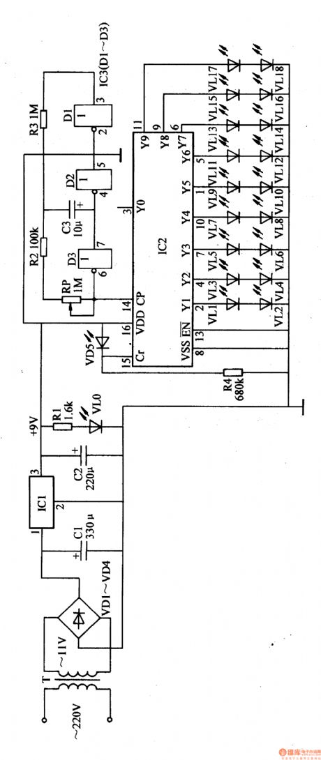
The optical controlled LED illuminations introduced here only works at night, and can be used as home decorations, shop’s ad lights or festival illuminations.
Working Principles:
As seen in the figure 1-168,the circuit consists of power circuit, optical controlled circuits, multivibrator and LED drive control circuit.
Alternating voltage 20Y can generate +9V voltate after works of T,VD1-VD4,C1 and IC1, which can be served as working power of IC2,IC3. Another current illuminates VL0 after being limited by R1.
In the daytime, VD5 is in low resistance state in light, and IC2 can't count because of 15 pin's high level. The YO terminal outputs high level, and Y1-Y9 output low level, so VL1-VL8 all don't illuminate. At night, VD5 is in high resistance state because of lack of light, so 15 pin becomes low level and IC2 begins to count. Multivibrator generates oscillate signals which can serve as IC2's 14 pin counting pulse, make IC2's YO-Y9 output high level one by one, and VL1-VL8 are illuminated one by one, showing the cycling light effect.
When we adjust RP's value, we can change the oscillate frequency of multivibrator, which can change the twinkle effect of the illuminations.
(View)
View full Circuit Diagram | Comments | Reading(749)
Sound Controlled LED Color Variable Illuminations
Published:2011/5/10 1:59:00 Author:Sue | Keyword: Sound Controlled, LED, Color Variable, Illuminations

Working Principle:
As seen in the figure, the sound controlled LED illuminations circuit consists of audio amplifying circuit, LED drive control circuit.
The audio amplifying circuit consists of BM,V1,V2,R1-R6,C1-C3 and RP.
LED drive control circuit consists of IC1-IC3,VL1-VL10 and R8.
Sensor BM put the audio signals which are amplified by V1,V2 onto IC1's 14 pin(CP terminal) as counting clock pulse. IC1's 3 pin(YO terminal), 2 pin(Y1 terminal) can provide IC2,IC3 with counting signal. Y2 terminal can provide 15 pin (resetting terminal) with resetting signal.
Among IC2,IC3's output terminals(YO-Y9 terminals) there are bicolored illuminated diode VL1-VL10. When IC2 and IC3 output high levels at the same time, the outside illuminated diodes will demonstrate orange color, or it will show red or green color.
As the space limited, the circuit only show VL1 and VL10 without VL2-VL9. And there is only one group of LED demonstrating circuits. When in practise, the numbers of illuminated diodes can be adjusted according to reality.
When we adjust the value of RP, we can change the level output to IC1's 14 pin, which will change the LED effect.
(View)
View full Circuit Diagram | Comments | Reading(1175)
LED Illuminations (3)
Published:2011/5/10 1:41:00 Author:Sue | Keyword: LED, Illuminations
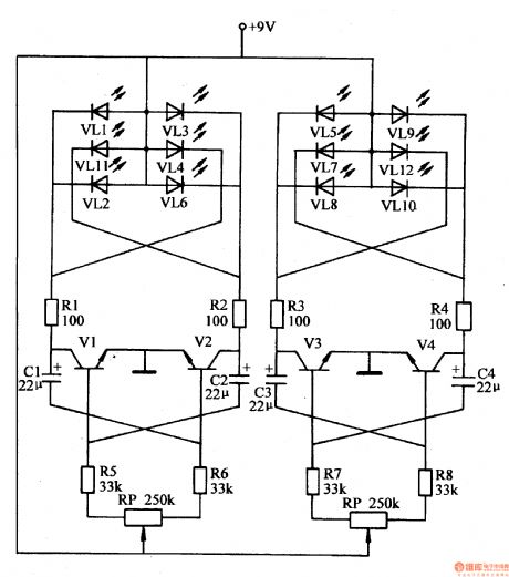
The LED illuminations introduced here have adjustable twinkle frequency and can make various kinds of lights patterns, and can also be used in toy decorations and gardening.
Working Principle:
As seen in the figure 1-159, the LED illuminations circuit consists of multivibrator A,B and illuminated diodes VL1-VL12.
Multivibrator A consists of resistor R5,R6, potentiometer RP1, capacitor C1,C2 and transistor V1,V2. Multivibrator B consists of resistor R7,R8, potentiometer RP2, capacitor C3,C4 and transistor V3,V4.
When A begins to work, R1,R2 will drive VL1-V to illuminate. When B begins to work, R3,R4 will drive VL5-VL12to illuminate.
When we adjust the values of RP and RP2, we can change the output waveform duty ratios of A and B respectively, so the light effect can be changed. (View)
View full Circuit Diagram | Comments | Reading(662)
LED Illuminations (2)
Published:2011/5/10 1:31:00 Author:Sue | Keyword: LED, Illuminations
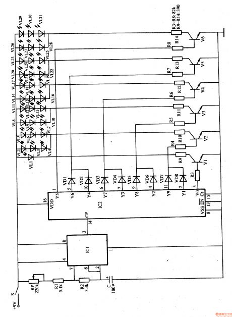
Working Principle:
As seen in the figure1-158, the circuit consists of multivibrator and LED drive control circuit.
The multivibrator circuit consists of potentiometer RP, resistor R1,R2, capacitor C and time base integrated circuit IC1.
LED drive control circuit consists of IC2、Vl-V6、VDl-VD8、R3-R14 and VLl-VL3l.
When power switch S is connected, multivibrator begins to work and provides IC2 with counting pulse signals. By this, IC2's YO-Y9 terminals output high level one by one, and make VL1-VL31 illuminated one by one.
When YO terminal outputs high level, V1 is connected, and VL1 is illuminated.
When Yl and Y9 terminal output high level, V2 is connected, and VL2-VL7 are illuminated.
When Y2 and Y8 terminal output high level, V3 is connected, and VL8-VLl3 are illuminated.
When W and Y6 terminal output high level, V5 is connected, and VL2O-VL25 are illuminated.
When Y5 terminal outputs high level, V6 is connected, and VL26-VL31 are illuminated.
In this circumstances, LED illuminations are illuminated one by one.
When we adjust RP's value, the illumination frequency can be changed. (View)
View full Circuit Diagram | Comments | Reading(619)
LED Illuminations (1)
Published:2011/5/10 1:18:00 Author:Sue | Keyword: LED, Illuminations
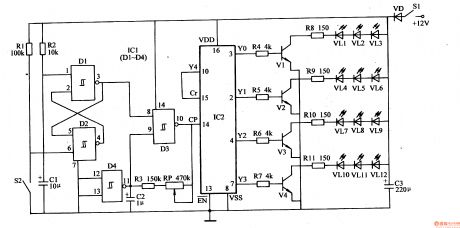
The LED illuminations introduced here can be used to make LED labels, motorcycle's lights and ambulance's signal lights.
Working principle:
As seen in the figure 1-157, the circuit consists of bistable trigger, clock oscillator and LED drive control circuit.
Bistable trigger circuit consists of resistor R1,R2, capacitor C1, switch S2 and four NAND gate Schimitt trigger integrated circuit IC1(D1-D4)'s inside D1,D2.
Clock oscillator consists of D3,C2,R3 and RP.
LED drive control circuit consists of IC2,R4-Rll,Vl-V4,C3 and VLl-VLl2.
When S1 is connected, +12V voltage provides the working power by S1 and VD.
When S2 is disconnected, bistable trigger output low level, and clock oscillator doesn't work, so the LED illuminations cannot show the effects. When S2 is connected, the bistable trigger reverses, and IC1 outputs high level which make oscillator begin to work, providing IC2's 14 pin(CP terminal) with counting pulse, and IC2's YO-Y4 terminal outputs cycling high level.
When YO terminal outputs high level, V1 is connected, VL1-VL3 are illuminated.
When Y1 terminal outputs high level, V2 is connected, VL4-VL6 are illuminated, while VL1-VL3 are put out.
When Y2 terminal outputs high level, V3 is connected, VL7-VL9 are illuminated, while VL4-VL6 are put out.
When Y3 terminal outputs high level, V4 is connected, VL10-VL12 ARE illuminated, while VL7-VL9 are put out.
When Y4 terminal outputs high lever, IC1 is forced to go back, and its YO terminal outputs high level again.
In this circumstances, the four LED illuminations are illuminated one by one and show the rotating effect.
If we adjust the value of RP, we can change the oscillate frequency of the clock oscillator, so the light rotating effect can be changed. (View)
View full Circuit Diagram | Comments | Reading(1063)
Pin functions and data of the integrated circuit
Published:2011/5/9 3:15:00 Author:TaoXi | Keyword: Pin functions, data
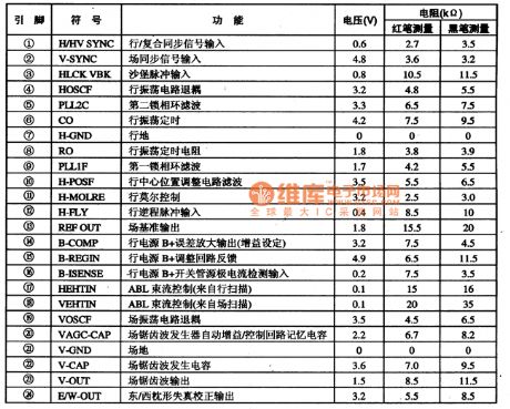
TDA9115--Multi-frequency multi-function processing integrated circuit
The TDA9115 multi-frequency multi-function processing integrated circuit is produced by the PHILIPS company that can be used in the new accounting computer monitor such as the Qinghua Tongfang 5E type color monitor.
1. The in-circuit block diagram
The TDA9115 has the line & field sync signal processing circuit, the line & field scanning small-signal processing circuit, the XRAY protection circuit, the I(2)C bus interface circuit, the VCO PLL circuit, the beam current control circuit, the line & field reference voltage circuit.etc. The integrated circuit is as shown in figure 37.
2.Pin functions and data
The TDA9115 is in the 32-pin double-row package, the pin functions and data is as shown in table 63.
Table 63 Pin functions and data of the integrated circuit
(View)
View full Circuit Diagram | Comments | Reading(547)
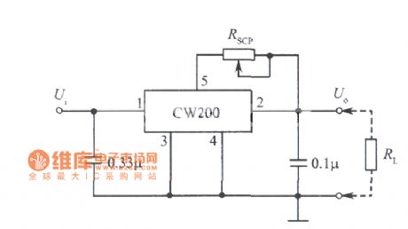
Adjustable constant current source circuit diagram composed of CW200
Published:2011/5/10 20:32:00 Author:Ecco | Keyword: Adjustable , constant current source
View full Circuit Diagram | Comments | Reading(1181)
Steper Motor Driver System Principle Circuit
Published:2011/5/7 20:42:00 Author:Robert | Keyword: Steper Motor, Driver System
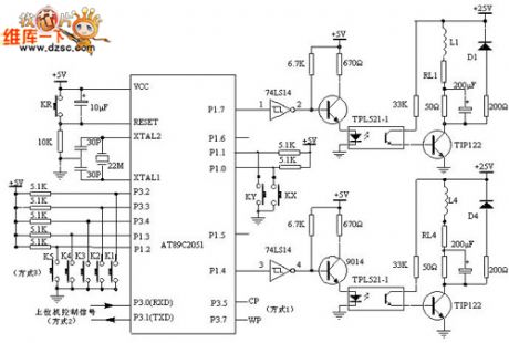
The steper motor driver system principle circuit is shown in the picture below.
The AT89C2051 outputs the control pulses from the P1's P1.4~P1.7 port, then these pulse signals are phase inverted by the 74LS14 to enter 9014, after its amplification these signals then control the photoelectric switch. After optical isolation, the pulse signals' voltage and current are amplified by the power tube TIP122 and then drive the stepper motor every phase windings. It would make the stepper motor have the corotation, reversion, acceleration, deceleration and stop movement with differential pulse signals. L1 shown in the picture is one phase winding of the stepper motor. The AT89C2051 is chosen to use 22MHz crystal. The purpose of using the high-frequency crystal is minimizing the influences on the PC pulse signal cycles by the AT89C2051 in mode 2.
The RL1~RL4 is winding resistance shown picture 1. The 50Ω resistance is a external resistance for current limiting, which is also a component to improve the loop circuit's time constant. D1~D4 are freewheeling diodes, which making the opposing electromotive force produced by motor winding be attenuated through them to protect the power tube TIP122 from damaged.
If the 50Ω external resistance is in parallel with a 200uF capacitor, it would improve the front of the current pulses which are transmitted to the stepper motor to improve the high-frequency performance of the stepper motor.
(View)
View full Circuit Diagram | Comments | Reading(1572)
using RDP-18 pyroelectric infrared control spotlight circuit
Published:2011/5/10 7:22:00 Author: | Keyword: pyroelectric infrared, control, spotlight

(View)
View full Circuit Diagram | Comments | Reading(522)
using P228 pyroelectric infrared control spotlight circuit
Published:2011/5/10 7:21:00 Author: | Keyword: pyroelectric infrared, control, spotlight

(View)
View full Circuit Diagram | Comments | Reading(518)
using HT76108 pyroelectric infrared control spotlight circuit
Published:2011/5/10 7:19:00 Author: | Keyword: pyroelectric infrared, control, spotlight

(View)
View full Circuit Diagram | Comments | Reading(599)
using BH9402 pyroelectric infrared control spotlight circuit
Published:2011/5/10 7:18:00 Author: | Keyword: pyroelectric infrared, control, spotlight

(View)
View full Circuit Diagram | Comments | Reading(482)
using CSl9508 pyroelectric infrared control spotlight circuit
Published:2011/5/10 7:17:00 Author: | Keyword: pyroelectric infrared, control, spotlight

(View)
View full Circuit Diagram | Comments | Reading(457)
using DH-03C pyroelectric infrared control delay spotlight circuit
Published:2011/5/9 9:21:00 Author: | Keyword: pyroelectric infrared , delay, spotlight

(View)
View full Circuit Diagram | Comments | Reading(454)
ABS Program Test Flow Circuit
Published:2011/5/10 7:40:00 Author:Robert | Keyword: ABS, Program Test Flow
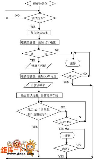
The ABS Program Test Flow Circuit is shown below.
(View)
View full Circuit Diagram | Comments | Reading(636)
TII Interface Circuit
Published:2011/5/9 19:18:00 Author:Robert | Keyword: TII, Interface
The TII Interface Circuit is shown below.
(View)
View full Circuit Diagram | Comments | Reading(584)
| Pages:1907/2234 At 2019011902190319041905190619071908190919101911191219131914191519161917191819191920Under 20 |
Circuit Categories
power supply circuit
Amplifier Circuit
Basic Circuit
LED and Light Circuit
Sensor Circuit
Signal Processing
Electrical Equipment Circuit
Control Circuit
Remote Control Circuit
A/D-D/A Converter Circuit
Audio Circuit
Measuring and Test Circuit
Communication Circuit
Computer-Related Circuit
555 Circuit
Automotive Circuit
Repairing Circuit