
Circuit Diagram
Index 444
RF2155 programmable plus power amplifier pin circuit
Published:2011/10/23 22:50:00 Author:May | Keyword: programmable, plus, power amplifier
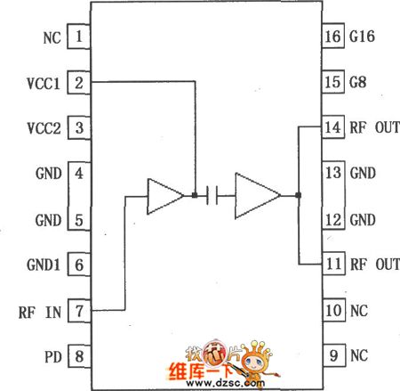
RF2155 is the programmable plus amplifier IC, and it is used in 3V handheld systems. It uses advanced GaAs heterojunction bipolar transistor (HBT), and it is designed for final linear RF amplification of analog cellular telephone system transmitter or applications with ISM working frequency 915MHz. Except outside match network, device itself includes power supply line. The two bits digital controlling offers 4 levels of power with 8dB per step. The pin array of RF2155 is shown in the diagram.
(View)
View full Circuit Diagram | Comments | Reading(938)
810 computer motherboard circuit diagram 01
Published:2011/10/26 1:53:00 Author:Ecco | Keyword: computer motherboard
View full Circuit Diagram | Comments | Reading(853)
810E computer motherboard circuit diagram 23
Published:2011/10/26 1:57:00 Author:Ecco | Keyword: computer motherboard

View full Circuit Diagram | Comments | Reading(798)
810E computer motherboard circuit diagram 22
Published:2011/10/26 1:56:00 Author:Ecco | Keyword: computer motherboard

View full Circuit Diagram | Comments | Reading(1377)
810E computer motherboard circuit diagram 21
Published:2011/10/26 2:00:00 Author:Ecco | Keyword: computer motherboard
View full Circuit Diagram | Comments | Reading(810)
810E computer motherboard circuit diagram 20
Published:2011/10/26 1:59:00 Author:Ecco | Keyword: computer motherboard

View full Circuit Diagram | Comments | Reading(792)
915MHz power amplifier application circuit composed of RF2155
Published:2011/10/24 1:23:00 Author:May | Keyword: 915MHz, power amplifier
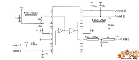
The diagram is 915MHz power amplifier application circuit composed of RF2155. Radio-frequency signal (RF) is input by pin 7, then it is output by pin 11 after enlarged by preamplifier and final power amplifier. Pin 7 and internal amplifierare directly coupled. So it is advised to add UHF blocking coupling capacitorto the out end of pin 7. Final power amplifier is mismatching collector transistor, output end of pin 11 and pin 14 is connected inside of the chip, pin 14 is used as final power amplifier supply side, it offers bias current to final power supply. Pin 14 is also used as thesecond harmonics filter circuit. It uses about 500mils transmission line as inductance. Pin 8 connects to power control foot (PC), and it can control this pin voltage thus control power. When voltage is low( 0V), amplifier power is in the open state; when voltage is inhigh level (3V), amplifier is in the total power working state.
(View)
View full Circuit Diagram | Comments | Reading(1314)
Small phone deconcentrator circuit
Published:2011/10/23 22:22:00 Author:May | Keyword: Small phone, deconcentrator
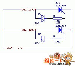
Working principleIfthe line connects totwo phones, which are separately connectedto L and L'. ( We know that when the phone is wating, the different of switch on office line L will have 60V or 48V DC voltage. When it is ringing, there is 95V or 75V AC voltage. When the phone is off-hook, the line voltage will drop to about 10V because the intervene of pnone internal resistance, this device is designed according to this principle. ) If there is phone now, AC current will ring through above-mentioned circuit diagram. If you want to turn to standy phone, the off-hook can dial number keylike standby phone ( attention: thephone must be in impulse dial state).
Components choose
BG1, B2are MCR100-6 small single-track SCRs, andthey require breakdown reverse voltage to begreater than 100V. D1, D2are 18V voltage regulator diodes. The whole cricuit can load in phone junction box.
(View)
View full Circuit Diagram | Comments | Reading(1395)
Photosensitive fuel gas annunciator circuit
Published:2011/10/23 21:56:00 Author:May | Keyword: Photosensitive, fuel gas, annunciator
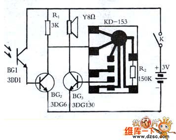
Fule gas can cook dinner and heat up water. During cooking process, thesoup overfolws, it's easy to put out , andfuel gas leak indoorcan cause a loss to life and property. Installing a fuel gas annunciator can avoid accident effectively.
Making material
3K, 150K 1/8 carbon-film resistor , one KD-153 music IC chip, one 3DDPhoto-Transistors, triode 3DG6, 3DG130, one8Ω speaker, switch, two dry batteries with battery clamp.
Working principle
When gas-cooker works normally, the annunciator is in the state of standby work. DG1 photistor receives flame shine, itpresents low resistance, BG2 breakovers, music vocal chip is in low level, speaker is not vocal. Once gas-cooker sudden dies out, photistor loses shine, its essential resistance increases, BG2gets saturation to close. (View)
View full Circuit Diagram | Comments | Reading(794)
RF2175 400MHz linear amplifier pin circuit
Published:2011/10/23 21:12:00 Author:May | Keyword: 400MHz, linear amplifier
RF2175 is high-power, high-performance linear amplifier IC which is applicated in 3V handheld systems, and ituses advanced GaAs heterojunction bipolar transistor ( HBT). It isintended for TERA handheld digital cellular system equipment's final stage linear RF amplification, band spread system and its working frequency is 380~512MHz. RF2175 has an analog bias control voltage to generate themaximal efficiency, and it includes 50Ω input and output, and it is easy to get best power, efficiency linear performance. RF2175 uses SSOP-16 plastic package, andits pin array is show in the diagram.
(View)
View full Circuit Diagram | Comments | Reading(930)
USA CDMA application circuit composed of RF2162
Published:2011/10/23 21:51:00 Author:May | Keyword: USA CDMA
The diagram is USA CDMA application circuit composed of RF2162. Radio-frequency signal (RF) isinput by pin 4, enlarged by preamplifier, final power amplifier, then output by pin 10, 11, 12. Pin 4 is directly coupling with inside amplifier, so itsuggests to add an UHF blocking coupling capacitor.Pin 13 is used as thesecond harmonics filter circuit, and it uses transmission line or inductanceandchip capacitor to make up filter with resonance at 2f0, it can offer low impedance path to second harmonics and short-circuit second harmonics effectively. Pin 14 is used as the final power amplifier power supply end, which offers bias current. Pin 5 connects to thefirst step enable voltage VREG1, when this pin is low level, the circuit shuts off; when it is inhigh level ( 2.8V),all circuit worksin thestandard state, and pin 5is connectedto 100pF high frequency filter capacitor. Pin 6 connects toanalog bias control pin VMODE, when pin 6 is 0V, itoffers theminimum bias.
(View)
View full Circuit Diagram | Comments | Reading(1707)
Password Electronic Switch Circuit Diagram
Published:2011/10/23 20:58:00 Author:May | Keyword: Password Electronic Switch
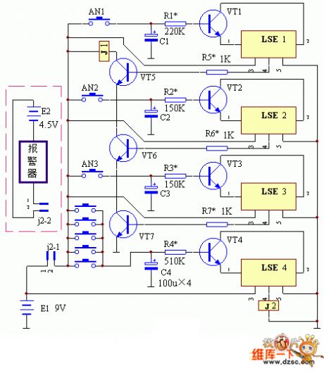
The working principle of this device is shown in the diagram. This password electronic switchhas three unlock buttons, and it also has the timelimiting circuit, error lock and electronic alarm circuit. It can make relay J1 excited pull in only by pressing unlock buttons AN1, AN2, AN3 correctly. The pick-up time is determined by the value of R1 and C1. In the diagram, transistors VT5, VT6, VT7 are cascaded into an AND gate circuit. When one of the three transistorsis cut off, the relay J1 will release. The five buttons AN1-AN8 are spliced into an OR gate logic circuit. It can cause the breaking over of transistor VT4. Then LSE's pin 1 and 2are broken over, and its pin 4 outputs high level, and relay J2 is excited and pulled in. Its locking time is determined by the value of R4 and C4.
(View)
View full Circuit Diagram | Comments | Reading(2246)
1880MHz Inside Collector Biased Amplifier Composed Of RF2324 Application Circuit
Published:2011/10/23 21:44:00 Author:May | Keyword: 1880MHz, Inside Collector Biased Amplifier
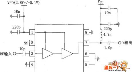
RF signals (RF) is input by pin 3 and output by pin 7 after enlarging by pre-amplifier and power amplifier. Pin 3 is directly coupled with internal amplifier. So, it adds a 10pF blocking coupling capacitor. The matching impedance is 50Ω when it works at 1880MHz. Pin 7 is output end of collector, whichcan connect power supply Vcc through choke or matching inductance. The typical matching impedance of this pin is 50Ω. In order to get the largest output power and efficiency, it connects to matching network outside to make the output impedance of amplifier match with it. Pin 1 is power down controlling end. The circuitworks when VPD=2.8V±0.1V (typical value of IPD is 8.5mA) and is closed when VPD<0.9V. VFD needs to add RF bypass circuit.
(View)
View full Circuit Diagram | Comments | Reading(735)
The circuit diagram of log amplifier
Published:2011/10/23 21:40:00 Author:May | Keyword: log amplifier

View full Circuit Diagram | Comments | Reading(1493)
Home-use fan IR remote control circuit
Published:2011/10/23 21:39:00 Author:May | Keyword: Home-use fan, IR remote control
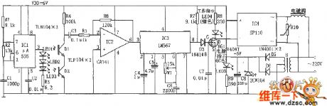
The diagram is home-use fan IR remote control circuit. This remote controller includes emitter and receiver controlling parts. The nucleus of IR emitter is an astable multivibrator which consists of 555 and R1, w1, c1, andits resonance frequency f=1.44/(R1+2Rw1)C1,whichis adjusted to 38KHz to drive infrared-emitting diode HG310 or HG450 and emit infrared pulse.
Infrared receiving tube should match to transmitting tube, and we should pay attention to light wave and light power. IC1 uses special infrared receiver manifold μPC1373HA to adjustthe L, C4 loop's center frequency in 38KHz, once it receives infrared light pulses, the signal is enlarged,detected,shapedby IC1to make IC1 output low level signal andBG2 stop accordingly, thenits collector outputs high level signal. (View)
View full Circuit Diagram | Comments | Reading(1578)
Wireless remote control electronic detonator circuit
Published:2011/10/23 21:32:00 Author:May | Keyword: Wireless remote control, electronic detonator
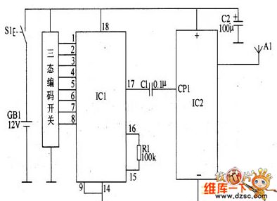
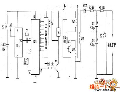
Circuit working principleThis wireless remote control electronic detonator circuit consists of wireless remote control transmitting circuit and wireless receiving detonating circuit.Wireless remote control transmitting circuit consists of control button S1, battery GB1, wireless encoding integrated circuit IC1, wireless transmitting integrated circuit IC2, resistor R1, transmitting aerial A1 and capacitors C1, C2, and it isshow in the diagram 1.
Wireless receiving detonation circuit consists of power switch S2(S2-1, S2-2), battery GB2, receive aerial A2, wireless receive intergared circuit IC3, wireless decode interated ciruit IC4; resistors R2-R6, capacitors C3-C5, transistors V1 and V2, relay K and transofrmer booster T, and it isshown in the diagram 8-28. Among them, A2, IC3, IC3, C3, R2, R3, VD1, V1 and K make up wireless receiving control circuit; R4, V2 and T make up oscillation voltage booster circuit; VD2, R5, C5 and R6 make up charge-discharge circuit.
(View)
View full Circuit Diagram | Comments | Reading(4966)
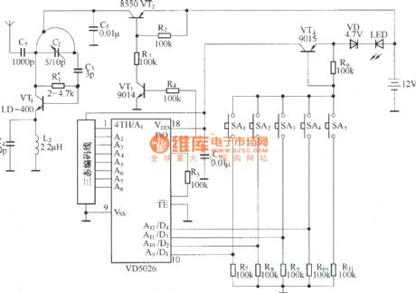
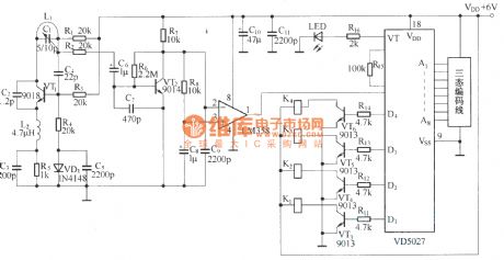
Fifth way wireless burglar alarm system (FDD5/JDD5) circuit diagram
Published:2011/10/20 1:50:00 Author:Rebekka | Keyword: Fifth way, wireless burglar alarm system
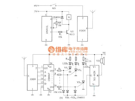
The picture(a) shows the code transmission circuit. FDD5 has set the digital coding circuit. It can be pre-encoded by encoder circuit, in use. As long as the connected components get power, it will automatically launch the emission signal. The picture(b) shows the remote control receiver decoding circuitry. JDD5 also integrated within the decoding circuit VD5027. (View)
View full Circuit Diagram | Comments | Reading(1222)
Numerical coding wireless remote control dimming circuit diagram
Published:2011/10/20 1:55:00 Author:Rebekka | Keyword: Numerical coding , wireless remote control dimming
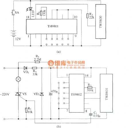
This circuit uses the wireless remote control component TWH630/TWH631 and encoding four dimming circuits TH9801/TH9802. It is composed of the wireless transmitter and receiver decoding controller. Pressing the transmitter button, you can control the brightness of incandescent lamps in accordance with the weak, medium, high, off. (A) is the transmitter circuit; (b) is the receiver circuit. (View)
View full Circuit Diagram | Comments | Reading(2634)
Four way remote control AC switching circuit diagram
Published:2011/9/28 4:33:00 Author:Rebekka | Keyword: Four way remote control, AC switching
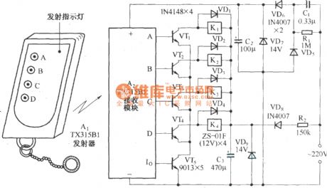
As shown, the circuit consists of TX315B1 type transmitter / receiver components to receive decoder circuit of four high output control signal. Driving through the transistor connected to four self-locking relay to AC power. Receive Groups pieces of the output of the A ~ D access VT1 ~ VT4 four relay driver tubes, each drive tube drives a self-locking relay output Io K. VT5 is formed by the emitter of VT1 ~ VT4 channel controller. Only when Io output signal decoding effective after the VT5 conduction, VT1 ~ VT4 are possible to conduct. (View)
View full Circuit Diagram | Comments | Reading(2861)
Four-channel interlock remote controller
Published:2011/10/19 22:58:00 Author:Rebekka | Keyword: Four-channel , interlock, remote controller
Four-channel remote interlock is composed oftransmitter and receiver.
Transmitter circuit diagram.
Receiver circuit diagram.
(View)
View full Circuit Diagram | Comments | Reading(2368)
| Pages:444/2234 At 20441442443444445446447448449450451452453454455456457458459460Under 20 |
Circuit Categories
power supply circuit
Amplifier Circuit
Basic Circuit
LED and Light Circuit
Sensor Circuit
Signal Processing
Electrical Equipment Circuit
Control Circuit
Remote Control Circuit
A/D-D/A Converter Circuit
Audio Circuit
Measuring and Test Circuit
Communication Circuit
Computer-Related Circuit
555 Circuit
Automotive Circuit
Repairing Circuit