
Circuit Diagram
Index 443
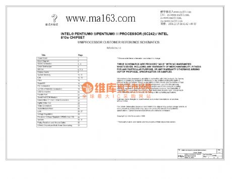
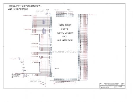
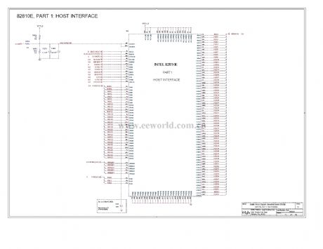
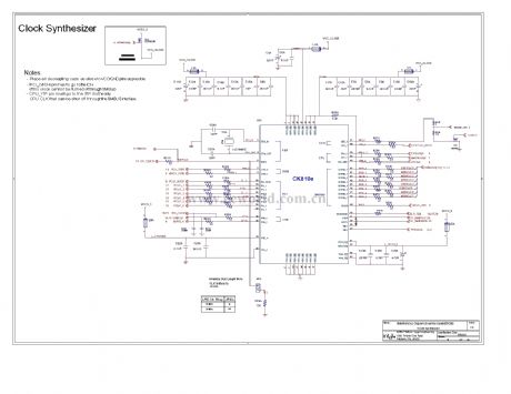
810E computer motherboard circuit diagram 01
Published:2011/10/27 1:36:00 Author:Ecco | Keyword: computer motherboard
View full Circuit Diagram | Comments | Reading(780)
805 cathode follower direct coupling power amplifier circuit
Published:2011/10/24 2:15:00 Author:May | Keyword: cathode follower, direct coupling, power amplifier

The practical situation is: due to the push tube's cathode minimum voltage is 0V, the practical 805 grid push range only has 0V~45V, at this time, in theoperating point namely the small triangle area, output power P0'=0.5(1425-1050)/(100-55)*1000 = 8.5W.
This is the biggest shortcoming of this type circuit. For low sensitivity sound box, it will lead to clipping distortion to turn the volume up. It is clearly that it can negligent if you never turn up so big volume. But if it only outputs 8.5W, the operating factor is so low. And the better choice is to adopt 300B. It is hard to achieve without minus gate voltage part if you want to get higher output power. (View)
View full Circuit Diagram | Comments | Reading(2617)
Icebox operating pilot lamp circuit
Published:2011/10/24 2:36:00 Author:May | Keyword: Icebox, operating pilot lamp
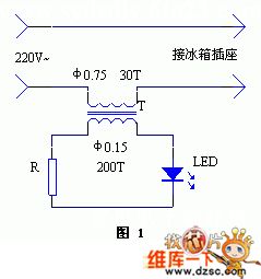
Installing operating light on the mains jack makes it convenient to watch icebox's starting and stoping, and can add the beauty to the mains jack to.
The circuit isshown asdiagram 1.It uses the secondaryinduced current of current transformerto lighten light-emitting diode.The current transformercan look for a slightly larger transistor radioinput or output transformer.And the data can bechanged according to the diagram. people should pay attention to winding-to-winding insulation. Current-limiting resistor R can be chosen in several to tens of ohm. (View)
View full Circuit Diagram | Comments | Reading(1026)
Frequency meter with 10Hz to 2MHz
Published:2011/8/22 20:31:00 Author:muriel | Keyword: Frequency meter , 10Hz to 2MHz
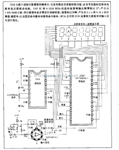
7208 seven metric system counter is used for frequency meter, it has latch and multiplexing function, and contains direct drive circuit and display driver circuit. 7207IC is divided the output frequencyof6.5536 MHz crystal oscillator by2 12which produces the 1600Hz square wave for calculator and display connection multiplexing. After fractional frequency, it produces 0.1 s and 0.01 s measurement gating signal and thenchooses communication and reset command pulse, modify ordered pulse. RCA company's 3130 operational amplifier is used for optimize the input signal. (View)
View full Circuit Diagram | Comments | Reading(3099)
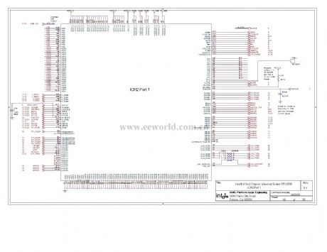
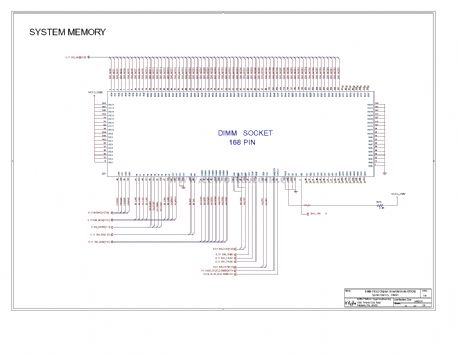
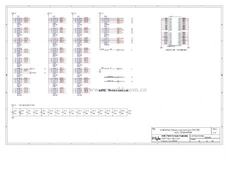
810 computer motherboard circuit diagram 13
Published:2011/10/25 21:57:00 Author:Ecco | Keyword: computer motherboard
View full Circuit Diagram | Comments | Reading(749)
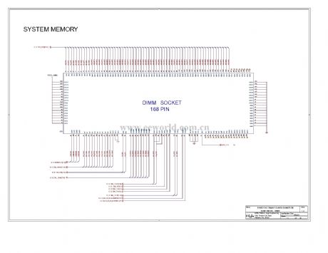
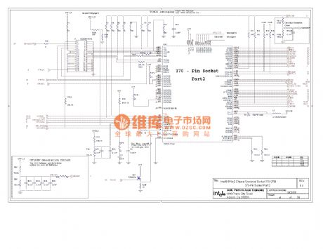
810 computer motherboard circuit diagram 12
Published:2011/10/25 21:56:00 Author:Ecco | Keyword: computer motherboard
View full Circuit Diagram | Comments | Reading(816)
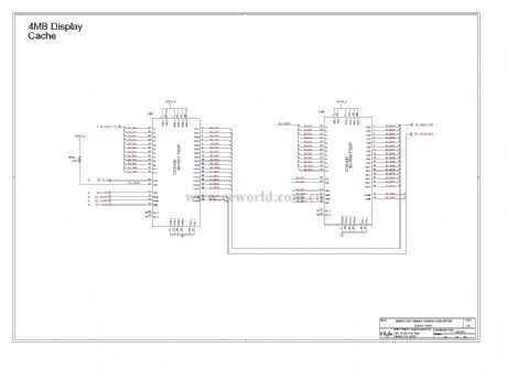
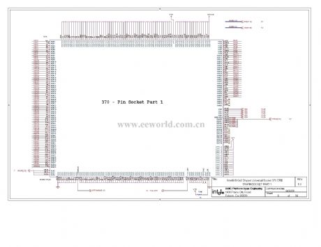
810 computer motherboard circuit diagram 11
Published:2011/10/25 21:55:00 Author:Ecco | Keyword: computer motherboard
View full Circuit Diagram | Comments | Reading(752)
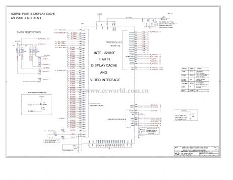
810 computer motherboard circuit diagram 10
Published:2011/10/25 21:54:00 Author:Ecco | Keyword: computer motherboard
View full Circuit Diagram | Comments | Reading(768)
810 computer motherboard circuit diagram 09
Published:2011/10/25 21:54:00 Author:Ecco | Keyword: computer motherboard
View full Circuit Diagram | Comments | Reading(840)
Application Circuit Design of Fuji IGBT Intelligence Module
Published:2011/8/22 21:15:00 Author:muriel | Keyword: Fuji IGBT, Intelligence module , application circuit design
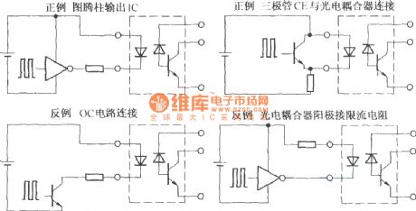
1.Photoelectric coupler drive circuit
Peripheral control circuit mainly aims at the single-chip control system of weak current control part, because the IPM module directly connects the distribution system, therefore, it must use segregation device to isolate the IPM module and the weak current circuit of control part, to protect the single-chip microcomputer control system. Meanwhile, the working conditions of IPM module depend largely on the right, effective and timely control signals. So,itdesigns a fine photoelectric coupler control circuit, whichis also the key to work normally IPM module, and it isshown as the chart.
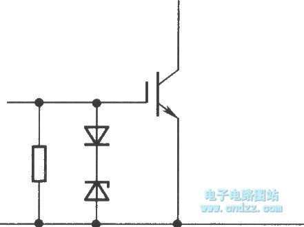
2.Buffer circuit
(View)
View full Circuit Diagram | Comments | Reading(941)
810 computer motherboard circuit diagram 08
Published:2011/10/25 21:53:00 Author:Ecco | Keyword: computer motherboard
View full Circuit Diagram | Comments | Reading(745)
810 computer motherboard circuit diagram 07
Published:2011/10/25 21:52:00 Author:Ecco | Keyword: computer motherboard
View full Circuit Diagram | Comments | Reading(788)
810 computer motherboard circuit diagram 06
Published:2011/10/26 1:43:00 Author:Ecco | Keyword: computer motherboard
View full Circuit Diagram | Comments | Reading(906)
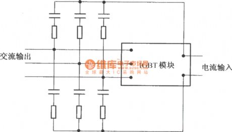
Grid overvoltage protection circuit
Published:2011/8/22 21:14:00 Author:muriel | Keyword: Grid , overvoltage protection circuit
Reasons for grid's overvoltage:
1. Static electricity on the grid capacitance cancause overvoltage.2. Capacitance mueller effect causes grid overvoltage.To prevent the IGBT grid-emitter from overvoltge, a resistance with dozen kilohm should be connected between the grid and emitter of IGBT in parallel. As the figure is shown, the resistance should beclosed to the grid and emitter. (View)
View full Circuit Diagram | Comments | Reading(1672)
The communication circuit of monitoring module and rectification module
Published:2011/8/22 21:16:00 Author:muriel | Keyword: monitoring module, rectification module
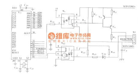
As shown is the monitoring module and rectification module of communication circuit. Optocoupler N9and N452 provide isolation between microprocessor D211 and rectification module, the N9 isisolated the send buffer V15 and V10, the send buffer V15 and V10 are designed for communcationdrive capability of 100 rectification module, N451 is a HG optocoupler buffer, it is receiving the rectification module's signals. (View)
View full Circuit Diagram | Comments | Reading(1297)
810 computer motherboard circuit diagram 02
Published:2011/10/26 1:54:00 Author:Ecco | Keyword: computer motherboard
View full Circuit Diagram | Comments | Reading(837)
810 computer motherboard circuit diagram 05
Published:2011/10/26 1:56:00 Author:Ecco | Keyword: computer motherboard
View full Circuit Diagram | Comments | Reading(761)
810 computer motherboard circuit diagram 04
Published:2011/10/26 1:55:00 Author:Ecco | Keyword: computer motherboard
View full Circuit Diagram | Comments | Reading(919)
810 computer motherboard circuit diagram 03
Published:2011/10/26 1:55:00 Author:Ecco | Keyword: computer motherboard
View full Circuit Diagram | Comments | Reading(811)
824~849MHz power amplifier circuit composed of RF2152
Published:2011/10/24 2:45:00 Author:May | Keyword: 824~849MHz, power amplifier
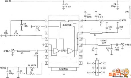
The diagram shows 824~849MHz power amplifier circuit composed of RF2152. Radio-frequency signal (RF) is input by pin 6, and it is output by pin 12 and 13 after enlarging by preamplifier and final amplifier. Pin 6 is directky coupling with internal amplifier, so it is added a blocking coupling capacitor in the pin 6. Output ends 12, 13, 14are connected to the chip, output matching network canmake amplifier output resistance match with it to get themaximum output power and efficiency. At the same time, pin 12, 13 are used as final power amplifier source supply's end, and it provides bias current through the pins.Pin 14 is used asthesecond harmonic's filter circuit. Pin 7 or 3 are connected to power control foot (PC) tocontrol this pin's voltage and source power. When voltage is inlow level (when 0.5V or lower), amplifier is in the offstate; when voltage is in high level (2.8V), amplifier power is in the standard working state. R3 and R4are usedfor bias adjustment.
(View)
View full Circuit Diagram | Comments | Reading(842)
| Pages:443/2234 At 20441442443444445446447448449450451452453454455456457458459460Under 20 |
Circuit Categories
power supply circuit
Amplifier Circuit
Basic Circuit
LED and Light Circuit
Sensor Circuit
Signal Processing
Electrical Equipment Circuit
Control Circuit
Remote Control Circuit
A/D-D/A Converter Circuit
Audio Circuit
Measuring and Test Circuit
Communication Circuit
Computer-Related Circuit
555 Circuit
Automotive Circuit
Repairing Circuit