
Analog Circuit
Index 2
An easy thermostat circuit composed of intelligent temperature sensor LM75 based on I2C Bus
Published:2011/9/8 5:38:00 Author:Felicity | Keyword: thermostat circuit, easy, intelligent temperature sensor
The figure shows an easy thermostat circuit composed of intelligent temperature sensor LM75 based on I2C Bus. LM75 drives the relay coil through 2N3904 transistor according to the test temperature to control the power supply of the thermostat to achieve thermostatic control. (View)
View full Circuit Diagram | Comments | Reading(1691)
Typical application of 7-way intelligent temperature sensor MAX6697
Published:2011/9/8 8:25:00 Author:Felicity | Keyword: 7-way, intelligent temperature sensor
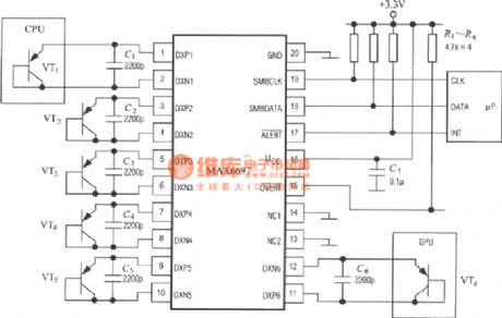
The figure shows the typical application circuit of 7-way intelligent temperature sensor MAX6697. MAX6697 matches 6 temperature measurement transistor (VT1~VT6). The transistors collector is closed to act as diode. VT1,VT6 are used to detect the chip temperature of CPU and GPU.C1~C6 and transistor in parallel can filter out the high frequency disturbance on the signal bus.C7 is power decoupling capacitor. R1~R4 are pull-up resistors.MAX6697 can connect to microprocessor (μP) through SMbus.
(View)
View full Circuit Diagram | Comments | Reading(926)
The low voltage logic circuit composed of intelligent temperature sensor TMP03
Published:2011/9/8 5:07:00 Author:Felicity | Keyword: low voltage logic circuit , intelligent temperature sensor
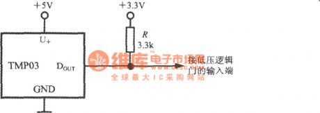
It’s convenient to drive logic gates under low voltage with the collector open. The low voltage logic circuit is shown in the figure. The DOUT terminal of TP03 connects to the +3.3V power through the 3.3kΩ pull-up resistor and the current through R is about 1mA. The output voltage of TMP03 is put on the input terminal of the low voltage logic gate. This circuit adapts +3.3V systems. (View)
View full Circuit Diagram | Comments | Reading(784)
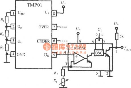
Using twisted pair to transmit temperature signal (low power programmable integrated temperature controller TMP01)
Published:2011/9/8 9:17:00 Author:Felicity | Keyword: twisted pair, temperature signal, low power, programmable integrated temperature controller
The output signal output by Pin 5 of TMP01 is analog voltage which can be easily disturbed during transmission in industrial sites. Then twisted pair can be adopted as shown in the figure. Firstly using OP297 split Uo into two-way signal and then transmitted through twisted pair and finally received and restored by AMP03. The differential amplifier composed by AMP03 can reduce the noise voltage as 95dB besides amplify the temperature signal. After restoration the lossless voltage signal Uo can be achieved.
(View)
View full Circuit Diagram | Comments | Reading(830)
Celsius or Fahrenheit temperature conversion circuit composed of cheap current output integrated temperature sensor TMP17
Published:2011/9/8 8:40:00 Author:Felicity | Keyword: temperature conversion, current output, output integrated temperature sensor
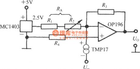
(View)
View full Circuit Diagram | Comments | Reading(1030)
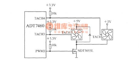
Using the PWM3 terminal of the intelligent remote hot fan controller ADT7460 to drive two three-wire fan
Published:2011/9/8 3:25:00 Author:Felicity | Keyword: PWM3 terminal, intelligent remote hot fan controller , three-wire fan
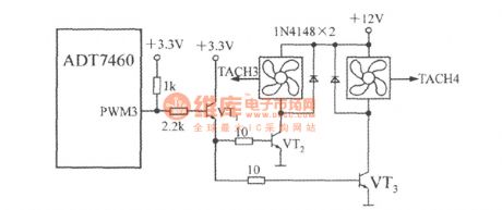
Using transistors:
Using FET:
(View)
View full Circuit Diagram | Comments | Reading(839)
smart humidity gauge constituted by the humidity sensor and the microprocessor circuit
Published:2011/8/31 1:52:00 Author:John | Keyword: smart humidity gauge, humidity sensor, microprocessor
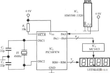
PIC16F874 has a wide range of supply voltage (+2.5 ~ +5 V), which is suitable for low voltage power supply. The quiescent current is less than 2mA. The RA port (RA0 ~ RA7) is the I / O interface. And the PA0 (also known as AIN0) port line is used to receive the voltage signal generated by the humidity sensor. Output bit PA1 ~ PA4 scans signal and receives inverting-phase drive signal through MC1413. Section between RB0 and RB6 of the RB port outputs 7-segment signal. And then the corresponding pen electrodes of LED display is within a ~ g. PIC16F874 also features of power-down protection. And MCLR reset the latch for the power-down side.
(View)
View full Circuit Diagram | Comments | Reading(1189)
Single-Phase Half-Wave Rectifier Circuit
Published:2011/8/23 23:41:00 Author:Robert | Keyword: Single, Phase, Half, Wave, Rectifier
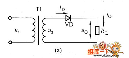
Common used low-power rectifier circuits has single-phase half-wave rectifier circuit, single-phase full-wave rectifier circuit and single-phase bridge rectifier circuit. Because the single-phase bridge rectifier circuit has good performance, it is one of the most common used rectifier circuits.The picture shows the single-phase half-wave rectifier circuit and working waveform. In the circuit shown in the picture, the transformer T1 would be convert the commercial electricity AC 220V U1 to the needed AC voltage U2. The rectifier diode VD would convert the transformer secondary voltage U2 to single-direction conducted DC voltage. (View)
View full Circuit Diagram | Comments | Reading(1391)
Single-Phase Full-Wave Rectifier Circuit
Published:2011/8/23 23:41:00 Author:Robert | Keyword: Single, Phase, Full, Wave, Rectifier
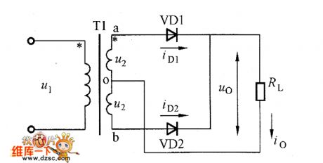
The picture shows the full-wave rectifier circuit and working waveform. From the circuit shown in the picture, we know that this circuit connects two rectifier diode to the transformer T1's secondary winding middle tap to make them work alternately. The * signal means the transformer's corresponding terminals. The transformer's two secondary voltage has the equal value. (View)
View full Circuit Diagram | Comments | Reading(1616)
Transistor Basic Voltage Regulator Circuit
Published:2011/8/23 23:40:00 Author:Robert | Keyword: Transistor, Basic, Voltage, Regulator
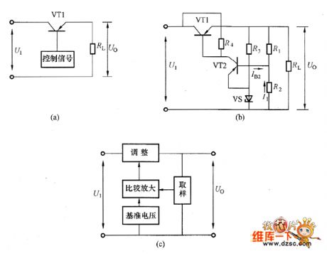
The transistors series voltage regulator circuit is shown in the picture. And, the picture (a) is equivalent circuit. The VT1 is adjustment transistor which is used to adjust the output voltage. The VT1 and load RL are in series. So this circuit is called the series voltage regulator circuit. Because the adjustment tube is using the transistors, the transistor series voltage regulator circuit could work under a big working current which could overcome the weakness that the zener diode regulator circuit's output current is limited by the zener diode limiting current. The picture (b) is the practical series voltage regulator circuit. The picture (c) is its diagram circuit. (View)
View full Circuit Diagram | Comments | Reading(1139)
Voltage Adjustable Circuit
Published:2011/8/23 23:41:00 Author:Robert | Keyword: Voltage, Adjustable
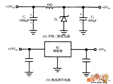
The modern mobile electronic devices is more easier to have this problem than the inchoate devices. In the communication devices and the FM radio, the oscillator voltage is controlled specially. The picture (a) shows the zener diode controller which is used in many car radio circuits. The picture (b) shows a three-segment voltage controller. It could control the mobile transmitter oscillator voltage in 10V. If these controlling components have errors, the circuit would have the frequency drifting. So that the nominal 12V car power is practically unstable. (View)
View full Circuit Diagram | Comments | Reading(731)
Grid Electrode Driving Circuit With Shortening Turn-Off Time
Published:2011/8/23 23:39:00 Author:Robert | Keyword: Grid, Electrode, Driving, Shorten, Turn-Off, Time
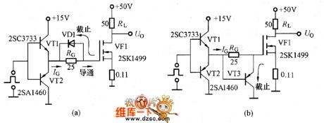
The picture shows the grid electrode driving circuit with shortening power MOSFET turn-off time. In the circuit shown in picture (a), the transistor VT1 and VT2 are make up the push-pull driving circuit with low output impedance. When the VF1 is conducted and the VD1 is disconnected, it would be through the grid resistance RG to charge the VF1's input capacitance Ciss. The RG limits its peak current. The VF1 turn-off time driving circuit would absorb the grid current and the diode VD1 would be conducted to short the RG. Thus the Ciss would discharge with a large current. So the electric charge stored in the grid electrode would be released rapidly.
The picture shows the grid electrode driving circuit with shortening turn-off time. (View)
View full Circuit Diagram | Comments | Reading(1215)
Push-Pull Switching Circuit With Grounding Source Electrode
Published:2011/8/23 23:39:00 Author:Robert | Keyword: Push-Pull, Switching, Grounding, Source, Electrode
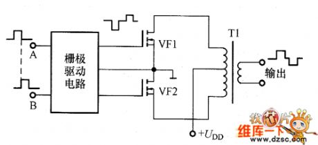
In the large-power applications it usually uses the push-pull switching circuit with transformer middle tapping method. The picture shows the common-used push-pull circuit with grounding source electrode. The push-pull switching circuit's input and output's phase difference is 180°. But the switching power controller has the A phase and the B phase which also have the 180° phase difference, it could directly drive the push-pull switching circuit composed of power MOSFET. Also in no-load case the power MOSFET in the circuit would have a high voltage between its drain electrode and source electrode which would easily have breakdown. So the power MOSFET's withstand voltage must have enough surplus capacity, and also it needs the absorbing circuit to limit the surge voltage. (View)
View full Circuit Diagram | Comments | Reading(796)
Transistor Disconnecting Circuit Using Inductance Stored Energy
Published:2011/8/23 23:39:00 Author:Robert | Keyword: Transistor, Disconnecting, Inductance, Stored, Energy
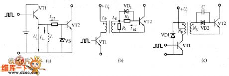
The picture shows the transistor disconnecting circuit using inductance stored energy. In the circuit shown in picture (a), during the transistor VT1 conducted time, the current IL, which is through the inductance L is IL, would change to be the peak current Ip after the VT1 conducting. Ip=U1TON/Lo. When the VT1 is disconnected, for keeping the current, the reverse current Ib2, which is through the VT2 base electrode, peak current would be Ip. This would accelerate the VT1's switching time. For this kind of circuit, because the reverse current Ib2 and the transistor conducted time TON are proportional, it would not get enough reverse current when the pulse is narrow. (View)
View full Circuit Diagram | Comments | Reading(693)
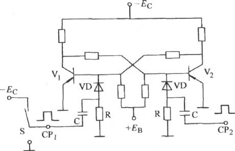
Bistable unilateral touching switch circuit
Published:2011/8/23 2:10:00 Author:Ecco | Keyword: Bistable , unilateral touching switch
View full Circuit Diagram | Comments | Reading(814)
Linear output integrated magnetic field sensor temperature compensation circuit
Published:2011/8/11 5:12:00 Author:John | Keyword: Linear output, integrated magnetic field sensor, temperature compensation
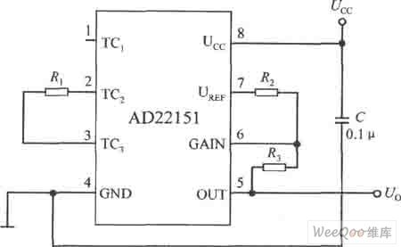
Constituted by the AD22151 bipolar mode temperature compensation circuit is as shown.
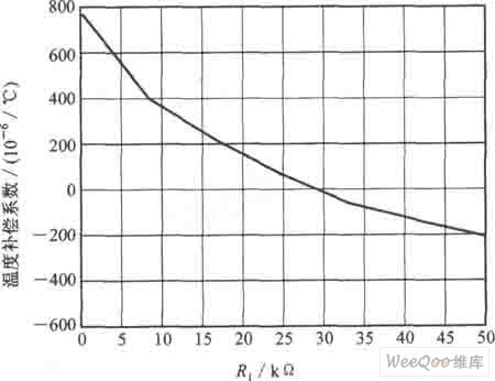
The circuit has the following characteristics: ① The temperature compensation resistor R1 is connected between the TC2 side and TC3 side; ② Zero magnetic field is biased on the UCC / 2; ③ It is able to compensate low temperature coefficient below the -500 × 10-6 / ℃. Under the bipolar mode, the curve between the resistance value of R1 and temperature compensation coefficient is shown. (View)
View full Circuit Diagram | Comments | Reading(1093)
Linear frequency output type humidity sensor and relative humidity measurement circuit
Published:2011/8/11 5:02:00 Author:John | Keyword: humidity sensor, relative humidity measurement
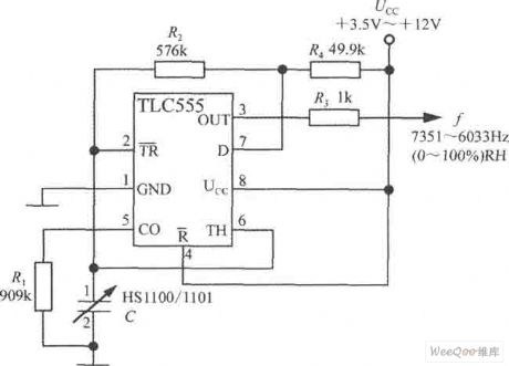
Linear frequency output type humidity sensor and relative humidity measurement circuit is as shown. The power supply voltage UCC ranges from +3.5V to +12 V. Utilizing a CMOS timer TLC555, HS1100/1101 and resistors R2 and R4 are coupled to constitute a monostable circuit. Then the relative humidity is converted into frequency signal. The output frequency ranges from 7351 Hz to 6033Hz and its corresponding relative humidity is from 0 to 100%. When RH = 55%, f equals to 6660Hz. Output frequency signals can be sent to the digital frequency meter or SCM system for measuring and displaying the relative humidity values. R3 is the current limiting resistor of the output end, ensuring the protective effect.
(View)
View full Circuit Diagram | Comments | Reading(2778)
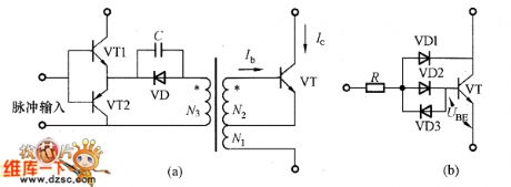
Narrow Pulse Driving Circuit
Published:2011/8/17 5:21:00 Author: | Keyword: Narrow, Pulse, Driving

The picture shows the circuit which could add enough reverse bias even for the narrow pulse. In the circuit shown in picture (a), when the VT1 is conducted, the current would be through R and VT3's base electrode. At the same time it would charge the capacitor C which is regarded as reverse bias power. If the VT1 is not conducted, the diode VD2 would make the VT2 conducted, the capacitor C's energy would be reversely added on the VD2's base electrode. If the carriers in VT2 are completely swept and over, it would reversely add the NSI's voltage on the VT3's base electrode through R2. For the circuit shown in picture (b), the reverse bias power C's voltage is also get from R2. The working principle is just the same with picture (a). (View)
View full Circuit Diagram | Comments | Reading(777)
Base Electrode Driving Circuit
Published:2011/8/13 7:52:00 Author:Robert | Keyword: Base Electrode, Driving
The base electrode driving circuit example is shown in the picture. When the base electrode current is big, to prevent the increasing of the storage time, it can use the Bekaa clamp circuit shown in picture (b). In the circuit, the base electrode current increases, when the transistor VT's saturation voltage is lower than UBE, the diode VD1 would be conducted. Thus it could prevent the increasing of the base electrode current. It is a circuit to prevent overexcitation.
The picture shows the base electrode driving circuit practical example.
(a)The drving circuit which the base electrode current is increasing as the ratio to the collector current.
(b)Bekaa clamp circuit. (View)
View full Circuit Diagram | Comments | Reading(827)
The circuit diagram of high precision and low offset current follower (LM11C, LF351)
Published:2011/8/8 22:11:00 Author:Felicity | Keyword: high precision, low offset, current follower
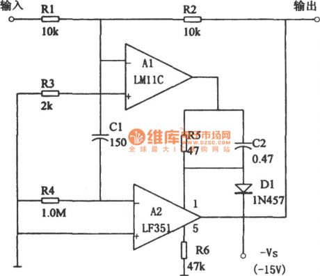
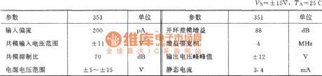
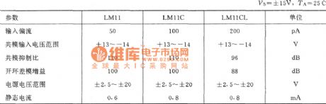
LM11C has a very low offset current (around 100pA), a low misalignment voltage( around 0.6 mV) and a 110dB CMRR.LF351 operational amplifier has a misalignment voltage about 10mv ,a static current around 3.4mA and a input offset current about 200PA. In this circuit, A2 adopts alternating-current coupling to reduce offset current. And this circuit has a long overload recovery time and the common-mode input voltage cannot exceed ±l0V. (View)
View full Circuit Diagram | Comments | Reading(994)
| Pages:2/24 1234567891011121314151617181920Under 20 |
Circuit Categories
power supply circuit
Amplifier Circuit
Basic Circuit
LED and Light Circuit
Sensor Circuit
Signal Processing
Electrical Equipment Circuit
Control Circuit
Remote Control Circuit
A/D-D/A Converter Circuit
Audio Circuit
Measuring and Test Circuit
Communication Circuit
Computer-Related Circuit
555 Circuit
Automotive Circuit
Repairing Circuit