
Analog Circuit
Index 8
EARTH_CONDUCTMTY
Published:2009/6/26 2:23:00 Author:May
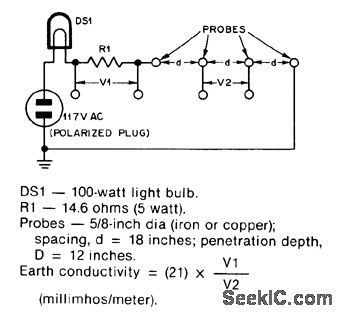
Simple AC measurement technique gives 25% accuracy, adequate for siting amateur radio antennas and designing radial ground systems. Measured values will range from 1 to 5 millimhos per meter for poor soil, 10-15 for average soil or flesh water,100 for very good soil, and 5000 for salt water.-J.Sevick, Short Grbund-Radial Systems for Short Verticals, QST,April 1978, p 30-33. (View)
View full Circuit Diagram | Comments | Reading(638)
ADD_ON_TRIGGERED_SWEEP
Published:2009/6/26 2:20:00 Author:May
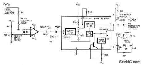
The circuit's input op amp triggers the timer, setting its flip-flop and cutting off its discharge transistor so that capacitor C can charge. When the capacitor voltage reaches the timer's control voltage (0.33Vcc), the flip-flop resets and the transistor conducts, discharging the capacitor. (View)
View full Circuit Diagram | Comments | Reading(780)
MONOSTABLE_CIRCUIT
Published:2009/6/26 1:54:00 Author:May
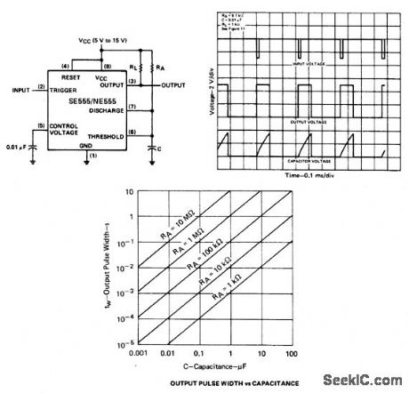
If the output is low, application of a negative-going pulse to the trigger input sets the flip-flop (Q goes low), drives the output high, and turns off 1. Capacitor C is then charged through Ra until the voltage across the capacitor reaches the threshold voltage of the threshold input. If the trigger input has returned to a high level, the output of the threshold comparator will reset the flip-flop (Q goes high), drive the output low, and discharge C through Q1. Monostable operations is initiated when the trigger input voltage falls below the trigger threshold. Once initiated, the sequence will complete only if the trigger input is high at the end of the timing interval. (View)
View full Circuit Diagram | Comments | Reading(849)
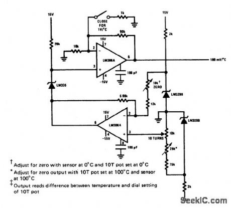
VARIABLE_OFFSET_THE_RMOMETER
Published:2009/6/26 1:42:00 Author:May
View full Circuit Diagram | Comments | Reading(636)
RF_BRIDGE_FOR_COAX
Published:2009/6/25 23:27:00 Author:May
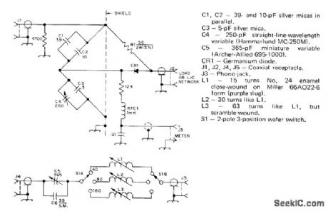
Simplifies adjustment of vertical antenna for 40, 80, and 160 meters.S1 in add-on LC unit switches coil for desited band. Values of C1-C4 and standard resistor R1 give range of 10 to 150 ohms for measurement of radiation resistance. Meter can be from 50 to 200μA full scale if 500 mW of power is available as signal source. For shorter-wavelength bands, change resistance in parallel with J1 to 5600 ohms and omit C6. L1 for 10 meters should then have 3 1/2 tums No. 18 spaced to occupy 1/4 inch on Miller4200 coilform. L2(15 meters) is Gtums No. 16 enamel closewound on similar form. L3 (20 meters) is 11 turns No.14 enamel on Miller 66A022-6 form.-J. Sevick, Simple RF Bridges, OST, April 1975, p 11-16 and 41. (View)
View full Circuit Diagram | Comments | Reading(0)
FET_CASCODE_VIDEO
Published:2009/6/25 22:22:00 Author:May
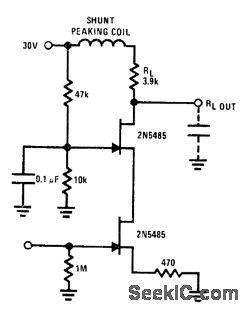
Use of 2N5485 FETs gives very low input loading, with feedback reduced almostto zero,Bandwidth of amplifier is limited only by load resistance and capacitance.-″FET Databook,″ National Semiconductor,Santa Clara,CA,1977、p 6-26-6-36 (View)
View full Circuit Diagram | Comments | Reading(775)
HIGH_TOGGLE_RATE_HIGH_FREQUENCY_ANALOG_SWITCH
Published:2009/6/25 21:49:00 Author:May
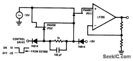
Commutator circuit provides low tmpedance gate drive to the PN4091 analog switch for both on and offdrive conditions.This circuit also approaches the ideal gate drive conditions for high frequency signal handling by providing a low ac impedance for off drive and high ac impedance for on drive to the PN4091 (View)
View full Circuit Diagram | Comments | Reading(0)
DTL_TTL_CONTROLLED_BUFFERED_ANALOG_SWITCH
Published:2009/6/25 21:48:00 Author:May
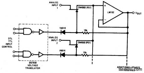
This analog switch uses the 2N4860 JFET for its 25 ohm ron and low leakage. The LM102 serves as a voltage buffer. This circuit can be adapted to a dual trace oscilloscope chopper. The DS7800 monolithic IC provides adequate switch drive controlled by DTL/TTL logic levels. (View)
View full Circuit Diagram | Comments | Reading(0)
TRIAC_TRIGGER
Published:2009/6/25 21:21:00 Author:May
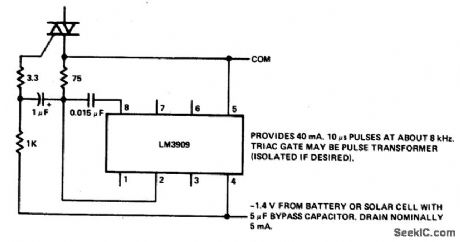
View full Circuit Diagram | Comments | Reading(0)
INDUCTORLESS_SWITCHING_REGULATOR
Published:2009/6/25 2:37:00 Author:May
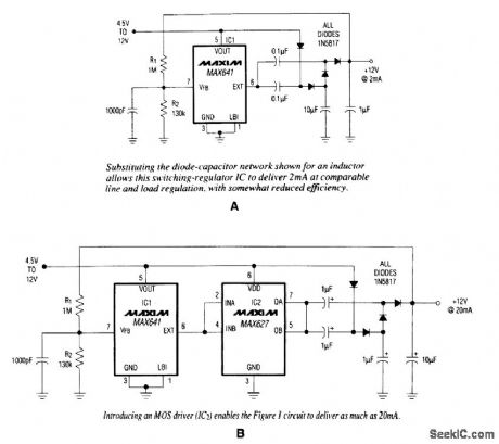
In conventional applications, switching-regulator ICs regulate 6,, by controlling the current through an external inductor. The IC in A, however, driving a diode-capacitor network in place of the inductor, offers comparable performance for small loads. The network can double, triple, or quadru-ple the input voltage.
Feedback from the R1/R2 voltage divider enables IC1 to set the regulated-output level. (As shown, the circuit derives 12 V from a 5- to 12-V input and provides as much as 2 mA of output cur-rent.) Adding a noninverting MOS driver (B) boosts the available output current to 20 mA. Substi-tuting the diode-capacitor network shown for an inductor allows this switching-regulator IC to deliver 2 mA at comparable line and load regulation, with somewhat reduced efficiency. (View)
View full Circuit Diagram | Comments | Reading(873)
AC_WITH_IMMUNITY_TO_LARGE_DC_OFFSET
Published:2009/6/24 23:29:00 Author:May
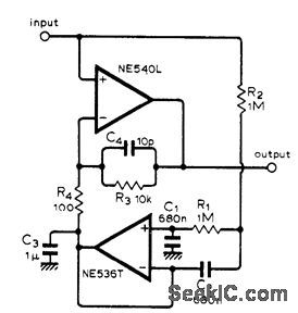
Designed to amplify from about 250 kHz down to Iow frequencies in presence of Iarge DC input offsets. Main NE540L ampllfier has gain of 101, while NE536T has DC gain of unity and forms part of Iow-pass network that applies DC input offset as common-mode voltage to inverting input of main amplifier.-A. Royston, Low Fre-quency A.C. Amplifier, Wireless World, May 1976, p 80. (View)
View full Circuit Diagram | Comments | Reading(745)
PHASE_SPLITTER_CIRCUIT
Published:2009/6/24 22:33:00 Author:May
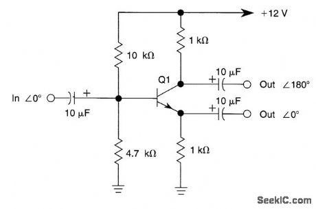
This phase splitter uses a 2N2222 (or other general purpose npn transistor) to achieve outputs that are 180° out ofphase. (View)
View full Circuit Diagram | Comments | Reading(2789)
PRECISION_PHOTODIODE_COMPARATOR_
Published:2009/6/24 22:31:00 Author:May
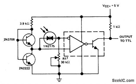
R1 sets the comparison level. At comparison, the photodiode has less than 5 mV across it, decreasing dark current by an order of magnitude. IC = LM 111/211/311. (View)
View full Circuit Diagram | Comments | Reading(857)
PRECISION_BATTERY_VOLTAGE_MONITOR_FOR_HTS
Published:2009/6/24 22:29:00 Author:May
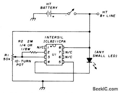
The precision voltage-monitor chip con-tains a temperature -compensated voltage ref-erence. R1 divides down the battery voltage to match the built-in reference voltage of IC1 (1.15 volts). When the voltage at pin 3 falls below 1.15 volts, pin 4 supplies a constant current of 7 mA to drive a small LED. About 0.2 LED) volt of hysteresis is added with R2. Without hysteresis, the LED could flicker on and off when the monitored voltage varies around the set point, as might be the case on voice peaks during receive. (View)
View full Circuit Diagram | Comments | Reading(704)
OPTICAL_COMMUNICATION_SYSTEM
Published:2009/6/24 22:28:00 Author:May
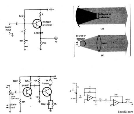
The simple modulator stage will accommodate most common LEDs. By adjusting the potentiometer, the bias ofthe transistor is varied until the LED is at its half output point.Then, audio will cause it to vary above and below this point. The purpose of R1 is to limit the current through the LED to a safe level and the purpose of the 10 ohm resistor is to allow a portion of the modulating signal to be observed on a scope. (View)
View full Circuit Diagram | Comments | Reading(0)
EQUIPMENT_ON_REMINDER
Published:2009/6/24 22:26:00 Author:May
Due to the low duty cycle of flashing LED, the average current drain is 1 mA or less. (View)
View full Circuit Diagram | Comments | Reading(641)
PEST_REPELLER
Published:2009/6/24 22:25:00 Author:May
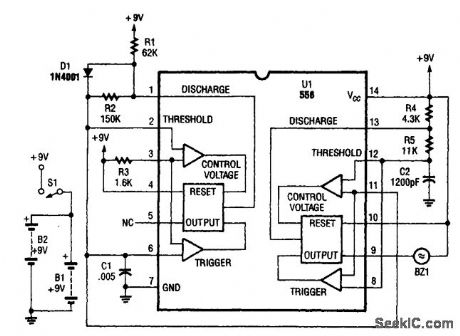
The two timers in the bug repeller have some interesting characteristics. Both of them have their thresholds externally set; the oscillator on the left has a 50% duty cycle and the oscillator on the right acts as a VCO. (View)
View full Circuit Diagram | Comments | Reading(1033)
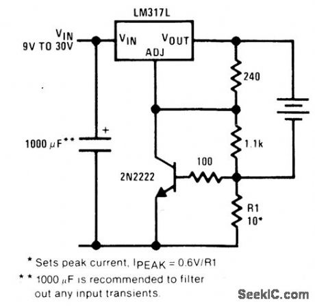
CURRENT_LIMITED_6_V_CHARGER
Published:2009/6/24 22:22:00 Author:May
View full Circuit Diagram | Comments | Reading(1)
NI_CAD_CHARGER
Published:2009/6/24 22:18:00 Author:May
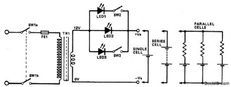
This circuit uses constant current LEDs to adjust charging current. It makes use of LEDs that pass a constant current of about 15 mA for an applied voltage range of 2-18 V. They can be paralleled to give any multiple of 15 mA and they light up when current is flowing. The circuit will charge a single cell at 15, 30 or 45 mA or cells in series up to the rated supply voltage limit (about 14 V). (View)
View full Circuit Diagram | Comments | Reading(760)
SIMPLE_SPECTRUM_ANALYZER_ADAPTOR_FOR_SCOPES
Published:2009/6/24 22:14:00 Author:May
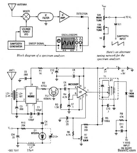
Suitable for monitoring an amateur band or a segment of the radio spectrurn, this simple adaptor uses an NE602 mixer-oscillator chip to produce a 455-kHz IF signal, which U2 amplifies, then feeds to detector D2 and the Y axis of an oscilloscope. VT is used to drive the horizontal axis input of a scope. L2 and L3 are coils suitable for the frequency range in use. For this circuit, coils are shown for the 10- to 15-MHz range. L2 and L3 are wound on Amidon Associates, T-37 or T-50 toroidal cores, and L1 is a commercial or homemade variable inductor, etc. (View)
View full Circuit Diagram | Comments | Reading(1785)
| Pages:8/24 1234567891011121314151617181920Under 20 |
Circuit Categories
power supply circuit
Amplifier Circuit
Basic Circuit
LED and Light Circuit
Sensor Circuit
Signal Processing
Electrical Equipment Circuit
Control Circuit
Remote Control Circuit
A/D-D/A Converter Circuit
Audio Circuit
Measuring and Test Circuit
Communication Circuit
Computer-Related Circuit
555 Circuit
Automotive Circuit
Repairing Circuit