
Analog Circuit
Index 9
ac_VOLTEMTER_HAS_UNIQUE_FEATURES
Published:2009/6/24 22:06:00 Author:May
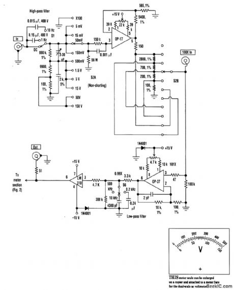
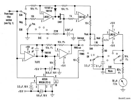
Though it's built with standard components, this ac voltmeter contains many features not typi-cally found in commercial meters; the most unusual is a selection of rectification modes. The meter responses available include true RMS ('fRMS), average, RMS-calibrated average responding, positive peak, negative peak, positive-peak hold, and negative-peak hold.High- and low-pass filters (S1 and S6, respectively) allow the -3-dB-passband to be varied from as little as 10 Hz to 200 Hz, to as wide as dc to 500 kHz. The low-pass filter also is effective in the 100x amplifier mode, where the input equivalent noise level is only 0.3 pV, with 10-kHz roll-off.
(View)
View full Circuit Diagram | Comments | Reading(3713)
SIMPLE_NI_CAD_BATTERY_CHARGER
Published:2009/6/24 22:00:00 Author:May
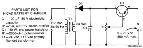
This circuit provides an adjustable output voltage up to 35 Vdc and maximum output current of 50 mA. Transistor Q1 dissipates quite a bit of heat and must be mounted on a heatsink. (View)
View full Circuit Diagram | Comments | Reading(693)
12_V_BATTERY_CHARGER
Published:2009/6/24 22:00:00 Author:May
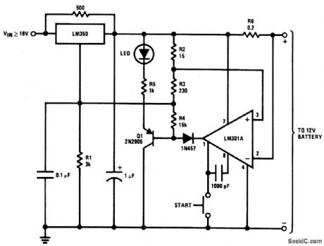
This circuit is a high performance charger for gelled electrolyte lead-acid batteries. Charger quickly recharges battery and shuts off at full charge. Initially, charging current is limited to 2A. As the battery voltage rises, current to the battery decreases, and when the current has decreased to 150 mA, the charger switches to a lower float voltage preventing overcharge. When the start switch is pushed, the output of the charger goes to 14.5V. As the battery approaches full charge, the charging current decreases and the output voltage is reduced from 14.5 V to about 12.5 V terminat-ing the charging. Transistor Q1 then lights the LED as a visual indication of full charge. (View)
View full Circuit Diagram | Comments | Reading(1)
HEADLIGHT_DELAY_UNIT
Published:2009/6/24 21:53:00 Author:May
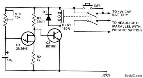
This circuit will operate a car's headlights for a predetermined time to light up the drive-way or path after the driver has left the car. SQ1 is pushed and Q2 is turned on closing the relay and turning on the car's headlights. C1 begins to charge through VR1 until Q1 turns on, turning Q2 off. The relay will then open switching off both the lights and the unit. The delay is governed by the time taken for the capacitor to charge, which is about one minute. (View)
View full Circuit Diagram | Comments | Reading(1483)
ICE_WARNING_AND_LIGHTS_REMINDER
Published:2009/6/24 21:50:00 Author:May
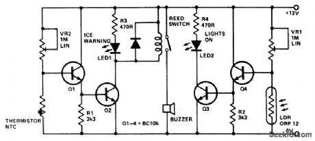
This device will tell a driver if his lights should be on and will warn him if the outside temperature is nearing zero by lighting a LED and sounding a buzzer9 VR1 adjusts sensitivity for temperature, VR2 for light. Both thermistor and LDR should be well protected. Most high gain NPN transistors will work. (View)
View full Circuit Diagram | Comments | Reading(754)
ADJUSTABLE_VIDEO_CABLE_EQUALIZER
Published:2009/6/24 21:49:00 Author:May
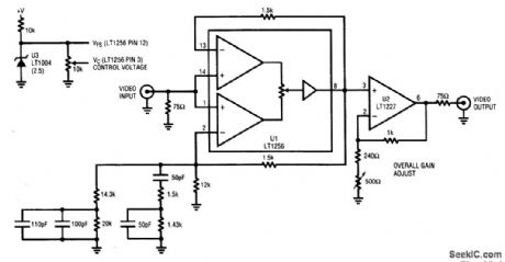
The figure is a complete schematic of the cable equalizer. The LT1256 (U1) is a two-input/one-output 40-MHz current feedback amplifier with a linear control circuit that sets the amount that each input contributes to the output. One amplifier (input pins 13 and 14) of the LT1256 is configured as a gain of one with no frequency equalization. The other amplifier (input pins 1 and 2) has frequency equalizing components in parallel with the 12-kΩ gain resistor. An additional amplifier (U2, LT1227) is used to set the overall gain. Two amplifiers were used here to make setting the gain a single ad-justment, but in a production circuit, the LT1256 can be configured to have the necessary gain and the whole function can be done with one chip. (View)
View full Circuit Diagram | Comments | Reading(920)
SIMPLE_VIDEO_GRAY_SCALE_GENERATOR_EUROPEAN_LINE_STANDARD
Published:2009/6/24 21:47:00 Author:May
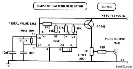
A simple gray-scale generator (staircase waveform) can be obtained with a CD4060 counter, a 1-MHz crystal oscillator, and several resistors to act as an elementary D/A converter to convert the binary count output to analog equivalent. This circuit is for European (PAL) standards. (View)
View full Circuit Diagram | Comments | Reading(2752)
ADJUSTABLE_VFO_TEMPERATURE_COMPENSATOR
Published:2009/6/24 21:45:00 Author:May
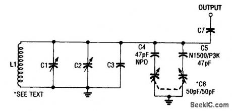
Use of a differential capacitor allows temperature compensation of LC circuit using an NPO and N1500 ceramic. C6 is a differential capacitor that has two stators and one common rotor. When one capacitance (stator) is maximum, the other is minimum. L1, C1, C2, and C3 are tuning, trimming, and fixed capacitors, respectively. (View)
View full Circuit Diagram | Comments | Reading(0)
VIDEO_CABLE_DRIVER
Published:2009/6/24 21:45:00 Author:May
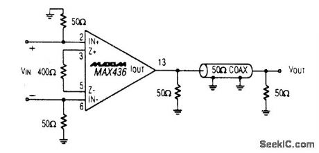
This is a MAX436 coaxial-cable driving circuit (View)
View full Circuit Diagram | Comments | Reading(0)
ANALOG_DEVICES
Published:2009/6/24 21:39:00 Author:May
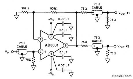
The AD8001 has been designed to offer outstanding performance as a video line driver. The im-portant specification of differential gain (0.01%) and differential phase (0.025°) meet the most ex-acting HDTV demands for driving one video load. The AD8001 also drives up to two back-terminated loads with equally impressive performance (0.01%, 0.07°). Another important consideration is isola-tion between loads in a multiple-load application. The AD8001 has more than 40 dB of isolation at 5 MHz when driving two 75-Ω terminated loads. (View)
View full Circuit Diagram | Comments | Reading(990)
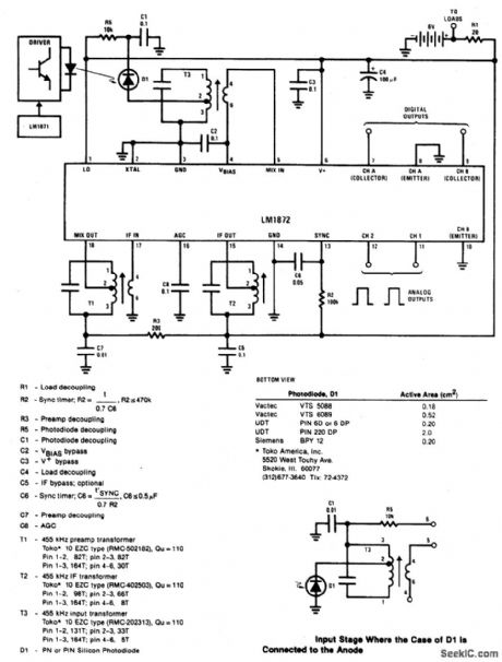
REMOTE_LOUDSPEAKER_VIA_IR_LINK
Published:2009/6/24 21:36:00 Author:May
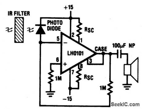
View full Circuit Diagram | Comments | Reading(687)
IR_TYPE_DATA_LINK
Published:2009/6/24 21:29:00 Author:May
View full Circuit Diagram | Comments | Reading(0)
ZERO_CENTER_INDICATOR_FOR_FM_RECEIVERS
Published:2009/6/24 21:26:00 Author:May
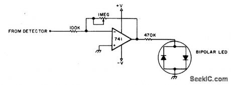
To adjust, tune in a station and adjust the 1 M pot for a null. Then ask the station to modulate and fine adjust so modulation peaks don't light the LEDs. Stations are properly tuned when neither LED is lit. (View)
View full Circuit Diagram | Comments | Reading(0)
FM_STEREO_TRANSMITTER
Published:2009/6/24 21:21:00 Author:May
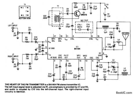
An FM stereo transmitter can be built around the BA1404 IC. This IC has all the functions necessary to generate an FM MPX signal. A separator oscillator circuit uses a 2N5210 transistor instead of the difficult-to-find 38-kHz crystal that is normally used. T1 is a 455-kHz IF transformer with 0.0039-μF capacitance added across it to enable tuning to 38 kHz. With this circuit, oscillator stabil-ity should be adequate. (View)
View full Circuit Diagram | Comments | Reading(0)
TEN_STEP_VOLTAGE_LEVEL_INDICATOR
Published:2009/6/24 21:21:00 Author:May
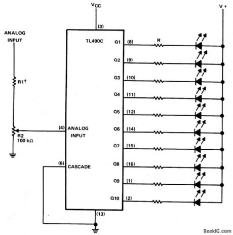
This ten-step adjustable analog level detector is capable of sinking up to 40 milliamperes at each output. The voltage range at the input pin should range from 0 to 2 volts. Circuits of this type are useful as liquid-level indicators, pressure indicators, and temperature tector dicators. They may also be used with a set of peres at active filters to provide a visual indication of input pin harmonic content of audio signals. (View)
View full Circuit Diagram | Comments | Reading(2560)
WIRELESS_MICROPHONE
Published:2009/6/24 21:20:00 Author:May
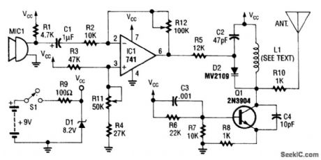
An op-amp IC (741) amplifies the audio signal from MIC1, and R12 controls its gain. Audio is fed to the oscillator circuit Q1 and related components. D2 is a varactor diode. Audio fed to D2 causes FM of the oscillator signal. L1 is 1/2 turns of #18 wire on a He diameter form. The antenna is a 12 whip. (View)
View full Circuit Diagram | Comments | Reading(0)
WIRELESS_GUITAR_TRANSMITTER
Published:2009/6/24 21:16:00 Author:May
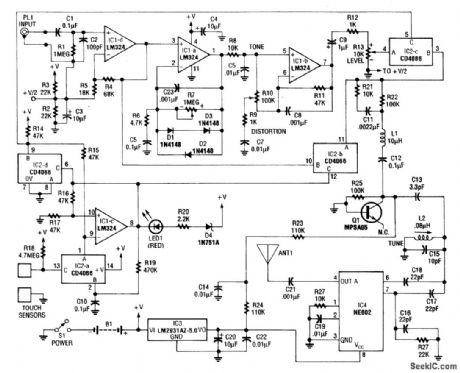
This transmitter has a built-in distortion effects unit and a touch switch to switch effects off and on. The circuit operates from a 9-V battery. IC1-a and IC1-b are used in the effects circuitry. IC1-d is an input preamp and IC2 is a quad analog switch to handle audio switching. Q1 acts as a varactor diode modulator while IC-4 is an 88- to 108-MHz FM oscillator. (View)
View full Circuit Diagram | Comments | Reading(0)
WIRE_TRACER
Published:2009/6/24 21:12:00 Author:May

This tracer works by placing a square-wave signal on the line to be traced. The square wave is rich in harmonics. A small transistor radio placed close to a wire carrying this signal will buzz. The ra-dio, therefore, is used as a probe to trace out the wire. (View)
View full Circuit Diagram | Comments | Reading(0)
CAPACITIVE_SENSOR_SYSTEM
Published:2009/6/24 21:08:00 Author:May
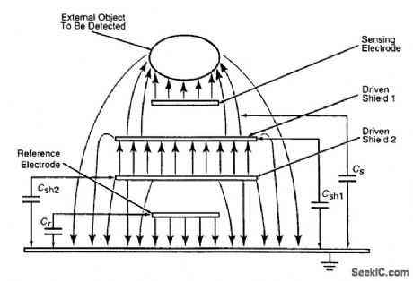
This figure illustrates the electric-field configuration of a capacitive proximity sensor of the ca-paciflector type. It includes a sensing electrode driven by an alternating voltage, which gives rise to an electric field in the vicinity of the electrode; an object that enters the electric field can be de-tected by its effect on the capacitance between the sensing electrode and electrical ground.Also, it includes a shielding electrode (in this case, driven shield 1), which is excited via a volt-age follower at the same voltage as that applied to the sensing electrode to concentrate more of the electric outward from the sensing electrode, increasing the sensitivity and range of the sensor. Be-cause the shielding electrode is driven via a voltage follower, it does not present a significant elec-trical load to the source of the alternating voltage.In this case, the layered electrode structure also includes a reference electrode adjacent to ground, plus a second shielding electrode (driven shield 2), which is excited via a voltage follower at the same voltage as that applied to the reference electrode. Driven shield 2 isolates the reference electrode from the electric field generated by driven shield 1 and the sensing electrode so that a nearby object exerts no ca[acitive effect on the reference electrode.The excitation is supplied by a crystal-controlled oscillator and applied to the sensing and ref-erence electrodes via a bridge circuit. Fixed capacitors C1 and C2 (or, alternatively, fixed resistors RI and R2) are chosen to balance the bridge; that is, to make the magnitude of the voltage at sens-ing-electrode node S equal the magnitude of the voltage at reference-electrode node R.The voltages at S and R are peak-detected and fed to a differential amplifier, which puts out volt-age 7, proportional to the difference between them. When no object intrudes into the electric field of the sensing electrode, the bridge remains in balance, and Vu - 0. When an object intrudes, it changes CS, unbalances the bridge, and causes Vu to differ from zero. The closer the object comes to the sensing electrode, the larger (Vu) becomes.An additional output voltage KVr is available, where K is the amplification and Vr is the voltage on the reference electrode. (View)
View full Circuit Diagram | Comments | Reading(0)
MICROPOWER_4_CHANNEL_SAMPLE_AND_HOLD_CIRCUIT
Published:2009/6/24 20:59:00 Author:May
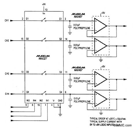
Three Maxim ICs make up this sample-and-hold circuit. The supply current is only 6μA. (View)
View full Circuit Diagram | Comments | Reading(0)
| Pages:9/24 1234567891011121314151617181920Under 20 |
Circuit Categories
power supply circuit
Amplifier Circuit
Basic Circuit
LED and Light Circuit
Sensor Circuit
Signal Processing
Electrical Equipment Circuit
Control Circuit
Remote Control Circuit
A/D-D/A Converter Circuit
Audio Circuit
Measuring and Test Circuit
Communication Circuit
Computer-Related Circuit
555 Circuit
Automotive Circuit
Repairing Circuit