
Analog Circuit
Index 15
PIEZOELECTRIC_DRIVER_CIRCUIT
Published:2009/6/23 2:59:00 Author:May
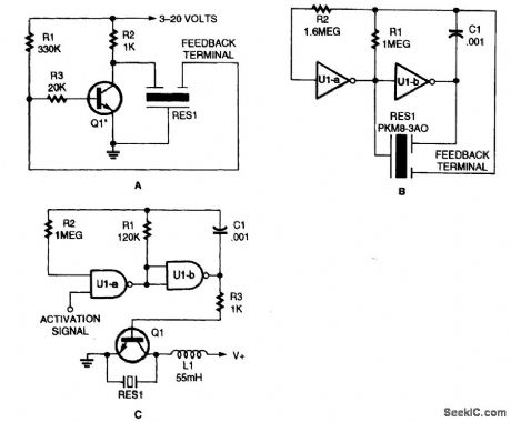
Three-terminal piezoelectric elements are typically driven by transistor circuits (A), or logic gates (B). Two-terminal devices can be driven by two NAND gates. A booster coil is used to compensate for the sound-pressure attenuation caused by the case. (View)
View full Circuit Diagram | Comments | Reading(1)
FET_MICROPHONE_MIXER
Published:2009/6/23 2:59:00 Author:May
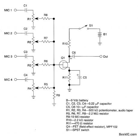
A JFET transistor is used as a high-to-low impedance converter and signal mixen Input impedance is approximately 500 kΩ but it can be increased by increasing R5 to R8 as high as 10 MΩ. Output Z is about 2 kΩ, but it can be increased or decreased by changing the value of R10 Use 560 or 680 Ω to feed a 600-Ω input; use 100 kΩ to 1 MΩ for high irnpedance. (View)
View full Circuit Diagram | Comments | Reading(1051)
CURRENT_BOOSTER
Published:2009/6/23 2:48:00 Author:May
View full Circuit Diagram | Comments | Reading(639)
CABLE_BOOTSTRAPPING
Published:2009/6/23 2:47:00 Author:May
Bootstrapping input shield for a follower reduces cable capacitance, leakage, and spurious voltages from cable flexing. Instability can be avoided with small capacitor on input. (View)
View full Circuit Diagram | Comments | Reading(819)
SAMPLING_RATE_PHASE_LOCK
Published:2009/6/23 2:44:00 Author:May
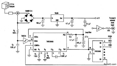


Most digital scopes have record lengths that are power of 2 (e.g., 1024 points) and sampling rates constrained to a 1-2-5 sequence. This can lead to measurement errors on power-line waveforms because an integral number of line cycles can't be captured. Digital scopes that calculate measurements, such as the rms level, across the entire record will be in error.One solution to this problem is to phase-lock the scope's sampling rate to the line frequency by exploiting the external clock input found on some digital scopes. Phase-locking the sampling to line frequency also tracks variations in the power-line frequency.A 9- or 12-Vac wall transformer provides the circuit's power and the frequency reference. The negative output of the diode bridge refines the circuit ground. The 78L05 regulator provides the +5 V supply for the three ICs. R3 and C2 create a low-pass filter on the half-cycles from one of the floating transformer outputs. R3 also limits the current into the internal diode clamps of the inverter gate.The inverter output becomes the power-line frequency reference and is one input (SIG in to the phase comparator) of the Signetics 74HC4046A phase-locked loop (PLL). The 74HC4040 divides the PLL output frequency by 1024 and feeds the divided clock back to the other PLL phase-comparator input (COMP in). The phase-comparator output (PC2) is filtered and drives the PLL's control voltage (VCO in) so that the output frequency is 1024 times the reference frequency.With the loop filter shown, the output frequency locks to the line frequency in about 10 s. The oscillator is locked to both 50- and 60-Hz inputs using a 74HC4046A and the values shown for resis-tors RI and R2 and capacitor C1.The output signal is buffered and sent to the scope's external clock input, which is typically a TTL-compatible input. A different tap from the 74HC4040 can be selected to control the number or cycles captured in one scope record. (View)
View full Circuit Diagram | Comments | Reading(1378)
MUTING_CIRCUIT
Published:2009/6/23 2:43:00 Author:May
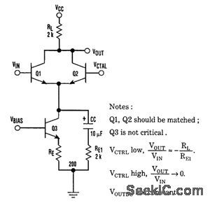
The circuit operates as follows: The signal is input to Vin and a dc control voltage is applied to VC. Vbias determines the desired bias point current. Assuming the following component and voltage values:
VCC=7.6 VdcVbias=1 VdcVin=1Vp-p,ac signal centered about 3.8 Vdc biasRL=2kΩRE=200kΩRE1=2kΩ
Q3 bias current is 1 mA, and dc output voltage is about 5.8Vwith an ac gain of about -1, Q1 and Q2 form a current switch and Q3 acts as a constant current source.For unmuted operation, Vc=0Vdc, and all of the bias current flows through Q1. Consequently, the circuit operates as a normal common emitter stage, with ac gain=-RL/RE1,. When Vc=5Vdc, all of the bias current flows through Q2, reducing the signal gain to zero. However, because the same dc current flows through RL, in both cases(unmuted and muted), the bias point at the output remains fixed. The Cc/RE1network is required to bypass the Q3 current source(which is a high impedance)to achieve alow ac impedance at the emitter of the Q1 common emitter stage during unmuted oper-ation. Cc is chosen to be a short circuit at signal frequencies of interest. The circuit works best if the Q1 and Q2 pair is matched. Typical change in the output dc voltage from unmuted to muted condi-tion is <5 mVdc.
RL,RE, and Vbias are chosen for desired dc operating conditions and signal dynamic range. Vbias, can be generated via a VCC voltage divider. The signal at Vin, can be ac coupled, but a bias circuit must be added to Q1's base to generate a dc component. RE1 is chosen for desired ac gain. Vin must be cen-tered about a dc component, and, to assure proper switching action, VCTRL, must be higher than Vin, by an amount greater than one VBE drop. (View)
View full Circuit Diagram | Comments | Reading(839)
SCOPE_VOLTAGE_CURSOR_ADAPTER
Published:2009/6/23 2:39:00 Author:May
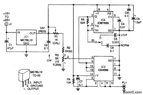
The voltage cursor adapter superimposes horizontal cursor lines on the top and bottom of the waveform-a kind of electronic calipers-to perrrtit direct readout of the voltage value. The cursor lines extend across the entire screen. The MC78L12 voltage regulator (IC1) supplies regulated 12 Vdc to the rest ofthe circuit. The ICM7555 timer (IC2) drives the CD4066B, a CMOS bilateral switch (IC3). This drive frequency can either be a normal frequency (NORM) of 100 Hz or a low-frequency (LO-F) of 10 kHz, depending on the setting of switch S1. Set S1 to LO-F for inputs below 500 Hz.The dc reference voltage supplied to pin 3 of IC3 is set by R3, a 10-turn, 5000-Ω precision potentiometen The voltage can be read directly from a turns counter dial coupled directly to the potentiometer's wiper. The accuracy of this reading can be 1% or better. Trimmer potentiometer R1 permits the voltage to R3 to be calibrated to precisely 10 V.The circuit is calibrated by setting the digital reading on the turns counter of R3 to the full clockwise position and adjusting R1 for a reading of 10 V at the wiper of R3 with a digital voltmeter.Bilateral switch IC3 converts the dc reference to a square wave with exactly the same wiper amplitude. The square-wave output appears on common pins 4, 9, and 10 of IC3 and coaxial plug PL1. (View)
View full Circuit Diagram | Comments | Reading(1060)
BOOTSTRAP_CIRCUIT
Published:2009/6/23 2:33:00 Author:May
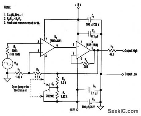
Bootstrapping the substrate of a JFET amplifier reduces the distortion caused by the nontinlearity of the JFET input capacitance. In the figure, a second feedback divider bootstraps the substrate of U1. With R1=500 kΩ (source im-pedance), THD at 10 kHz was reduced an order of magnitude. (View)
View full Circuit Diagram | Comments | Reading(1576)
HF_VFO_CIRCUIT
Published:2009/6/23 2:22:00 Author:May
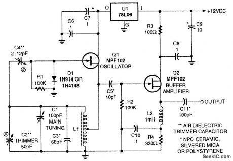
This typical HF VFO circuit has several stability-enhancing features, including well-chosen capacitor types. The frequency of the VFO is approximately 2π (C1 + C2 + C3) L1. L1 should be an aircore type coil, rigidly mounted, with high (>200 value) value of Q. (View)
View full Circuit Diagram | Comments | Reading(0)
CAPACITOR_HYSTERESIS_COMPENSATOR
Published:2009/6/23 2:22:00 Author:May

View full Circuit Diagram | Comments | Reading(0)
PULSE_ECHO_DRIVER
Published:2009/6/23 2:19:00 Author:May
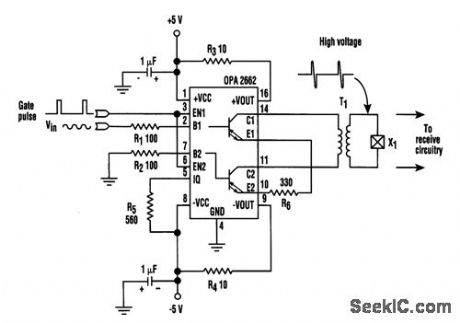
This pulse-echo driver uses the OPA2662 dual operational transconductance amplifier(OTA)from Burr-Brown(the reeeive circuitry isn't shown). The OTA is preferable over an op amp for driv-ing low impedances because it provides a current output rather than a voltage output.Ultrasonic pulse-echo applications often incorporate a transformer-coupled crystal to obtain a high-voltage pulse because the echo can be orders of magnitude smaller in amplitude. The trans-former turns ratio also provides tuning at the resonant frequency of the crystal, which usually means a relatively low-impedance primary winding.An operational transconductance amplifier(OTA)is preferred over an op amp to drive such a low impedance. One particular application involves a pulse-echo driver circuit using the OPA2662. (View)
View full Circuit Diagram | Comments | Reading(1596)
OCTAVE_EQUALIZER
Published:2009/6/23 2:18:00 Author:May
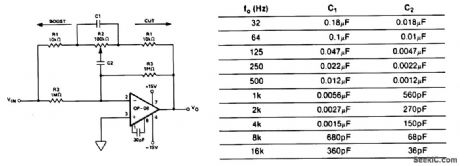
This circuit is one section of an octave equalizer used in audio systems. The table shows the val-ues of C1 and C2 that are needed to achieve the given center frequencies. This circuit is capable of 12 dB boost or cut, as determined by the position of R2. Because of the low input bias current of th,e OP-08, the resistors could be scaled up by a factor of 10, and thereby reduce the values of C1 and C2 at the low-frequency end. In addition, 10 sections will only draw a combined supply current of 6 mA maximum. (View)
View full Circuit Diagram | Comments | Reading(929)
JFET_CHOPPER_CIRCUIT
Published:2009/6/23 2:14:00 Author:May
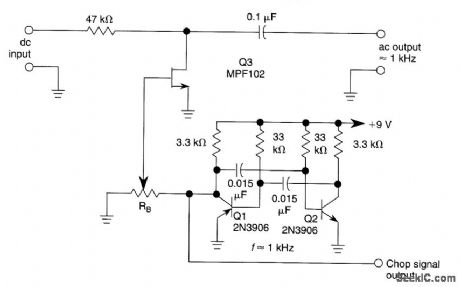
A JFET (MPF102) is used to chop a dc signal for amplification in an ac coupled amplifien Q3 is the chopper element and Q1-Q2 forms the multivibrator to derive a chopping signal. R, sets the bias on the FET to keep the drive to MPF102 as low as possible. (View)
View full Circuit Diagram | Comments | Reading(2339)
POWER_BOOSTER
Published:2009/6/23 1:57:00 Author:May
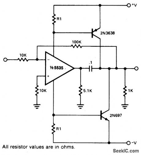
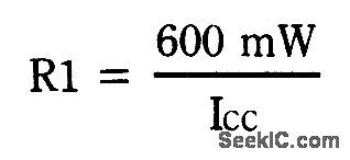
Power booster is capable of driving mod-erate loads. The circuit as shown uses a NE5535 device. Other amplifiers may be sub-stituted only if R1 values are changed because of the ICC current required by the amplifier. R1 should be calculated from the following ex-pression: (View)
View full Circuit Diagram | Comments | Reading(0)
ac_LINE_VOLTAGE_BOOSTER
Published:2009/6/23 1:54:00 Author:May
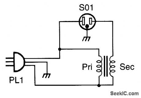
When incoming ac power drops, you can bring the voltage back up with this booster circuit. It adds the transformer's secondary voltage to the ac line voltage. (View)
View full Circuit Diagram | Comments | Reading(1403)
dc_OUTPUT_CHOPPER
Published:2009/6/23 1:49:00 Author:May
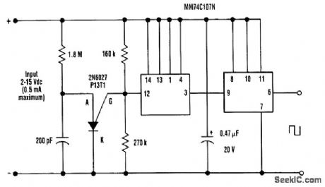
Any dc voltage source in the 2- to 15-V range can be chopped into a unipolar square wave that has a peak amplitude nearly equal to the dc source voltage with circuit (lightly loaded CMOS will swing within a few millivolts of each rail at low frequencies). Depending on the actual voltage of the supply, the programmable-unij unction-transist or (PUT) relaxation oscillator produces 2000-Hz trigger pulses. These pulses operate the cascaded 74C107 flip-flop, producing a square wave. (View)
View full Circuit Diagram | Comments | Reading(0)
SUBAUDIBLE_TONE_ENCODER
Published:2009/6/23 1:48:00 Author:May
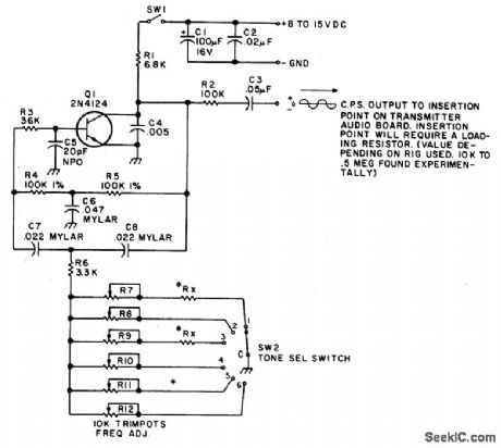
This twin-T oscillator produces six preset subaudible tones from 93 to 170 Hz in three ranges. (View)
View full Circuit Diagram | Comments | Reading(0)
VARIABLE_FREQUENCY_ASTABLE_II
Published:2009/6/23 1:43:00 Author:May
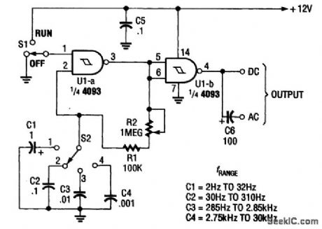
This circuit uses a single potentiometer and switched capacitors to cover 2 Hz to 30 kHz。 (View)
View full Circuit Diagram | Comments | Reading(0)
VARIABLE_FREQUENCY_ASTABLE_I
Published:2009/6/23 1:37:00 Author:May
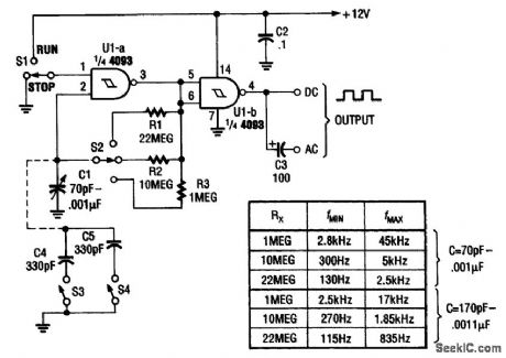
This Circuit is a variable frequency oscillator usming a trimmer capacitor or a three-gauge AM broadcast capacitor salvaged from an old AM radio. The there sections must be paralleled. (View)
View full Circuit Diagram | Comments | Reading(981)
CW_SIGNAL_PROCESSOR
Published:2009/6/23 1:36:00 Author:May
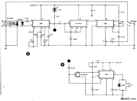
This circuit provides interferenced rejection for the CW operator. The 567 phase-locked loop is configured to respond to tones from 500 to 1100 Hz. The Schmitt trigger reduces the weighting effect caused by the output of the PLL remaining low after removal o f the audio signal. Ten to 15 millivolts of audio activate the circuit. For periods of loss of signal, circuit B will automatically switch back to live receiver audio after a suitable delay. (If a relay with a 5-volt coil is not available, the circuit can also be powered from +12 volts.) When circuit B is used, the contacts on relay K1 replace S1. (View)
View full Circuit Diagram | Comments | Reading(1164)
| Pages:15/24 1234567891011121314151617181920Under 20 |
Circuit Categories
power supply circuit
Amplifier Circuit
Basic Circuit
LED and Light Circuit
Sensor Circuit
Signal Processing
Electrical Equipment Circuit
Control Circuit
Remote Control Circuit
A/D-D/A Converter Circuit
Audio Circuit
Measuring and Test Circuit
Communication Circuit
Computer-Related Circuit
555 Circuit
Automotive Circuit
Repairing Circuit