
Analog Circuit
Index 6
PIN_DIGDE_ATTENUATOR
Published:2009/6/28 22:51:00 Author:May
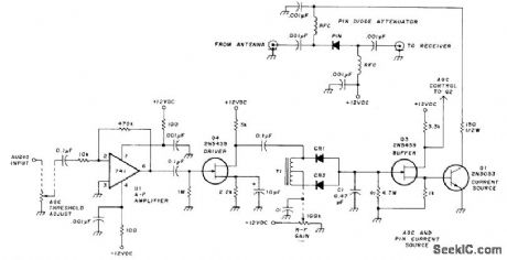
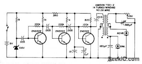
Designed for insertion between antenna and input of any HF receiver to improve adjacent-channel selectivity by providing attenuation ahead of mixer for entire tuning range. Hewlett-Packard 5082-3379 PIN diode has very low impedance when conducting and very high impedance when biascurrent is small. NPN transistor Q1 provides over 100 mA as current source to PIN diode. Q1 is driven by AGO circuit through JFET buffer Q3.AGC voltage is derived from top of audio gain control in receiver for rectification, with 200 mVRMS at input of opamp U1 giving maximum attenuation. Center tap of T1 (any small AF transformer) can be grounded. CR1 and CR2 are germanium diodes. Article also gives circuit of IF system using cascaded 9-MHz crystal filters to improve selectivity further and provide over all AGC control range of 70 dB.-M. Goldstein, Improved Receiver Selectivity and Gain Control, Ham Radio, Nov. 1977, p 71-73. (View)
View full Circuit Diagram | Comments | Reading(1880)
ACTIVE_ANTENNA
Published:2009/6/28 22:41:00 Author:May
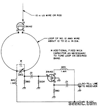
Uses tuned loop with relatively low a for broadband operation over one amateur band, phase-coupled by FET to 10-inch vertical sensing antenna to give unidirectional reception pattern. Loop is tuned to either 80 or 40 meters by trimmer capacitor at its base. Out.put of loop is coupled to another 3N142 FET used as source follower, to isolate output of loop from heavy loading eff ect of 50-ohm transmission line going to receiver. Performance is comparable to that of full-size quarter-wave vertical antenna on 40 meters. Battery source can be used because drain is only about 2 mA.-J. J. Schultz, An Experimental Miniature Antenna for 40 to 80 m, 73 Magazine, June 1973, p29-32. (View)
View full Circuit Diagram | Comments | Reading(0)
144_MHz_FOR_VSWR_BRlDGE
Published:2009/6/28 22:32:00 Author:May
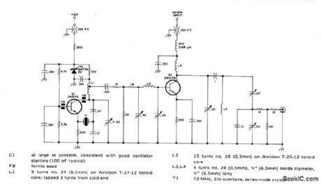
Modulated signal source provides 10-mW CW output and 5mW modulated output at modulation frequency of 1000 Hz. Spurious and harmonic outputs are 40 dB below desired output. 72-MHzcrystal oscillator is followed by doubler stage. attenuation between generator and load. Use Oscillator runs continuously while doubler is regulated power supply or batteries.-J. flei-keyed whh simple ON/OFF square-wave keying, Freedom from load variations is obtained with double-tuned output filter providing up to 6-dB attenuation between generator and load, Use regulated power supply or batteries.-J.Reisert, Matching Techniques for VHF/UHF Antennas, Ham Radio, July 1976, p 50-56. (View)
View full Circuit Diagram | Comments | Reading(848)
LOOP_PREAMP
Published:2009/6/28 22:31:00 Author:May
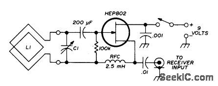
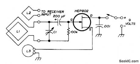
Loop for lower-frequency amateur bands is connected to gate of HEP802 FET and output to receiver istaken from FET source.C1 is two-gang variable capacitor from old broadcast radio, with stators in parallel to give 600 pF. Article gives loopdata for 40, 80, and 160 meters and for high end of broadcast band. For 40 and 80 meters, use 18-inch square loop with 2 tums spaced 1/4 inch. Ground lower end of 100K resistor to provide ground retum for FET.-K. Comell, Loop Antenna Receiving Aid, Ham Radio, May 1975, p 66-70. (View)
View full Circuit Diagram | Comments | Reading(1185)
RF_NOISE_BRIDGE
Published:2009/6/28 22:30:00 Author:May
Improves accuracy and measurement range for impedance measurements from 3.5 to 30 MHz, particularly resistive and reactive components of high-frequency antennas. Accuracy is 3 ohms BMS. Wideband noise, generated in zener followed by threetransistor amplifier, is iniected into two legs of bridge in equal amounts by toroidal transformer having quadrifilar windings. With un known impedance connected and detectorlany communication receiver) set to desired frequency, reference impedances (250-ohm noninductive pot and 360-pF variable capacitor) are adjusted for deepest possible null. Value of unknown impedance is then equal to parallel combination of references. Article covers construction and calibration.-R. A. Hubbs and A. F.Doting, Improvements to the nx Noise Bridge, Ham Radio, Feb. 1977, p 10-20. (View)
View full Circuit Diagram | Comments | Reading(4271)
Q_MULTIPLIER_FOR_LOOP
Published:2009/6/28 22:20:00 Author:May
Improves performance of loop antenna on 40,80, and 160 meters. Feedback control is obtained with adjustable single-turn loop L3 coupled to L1, and receiver input is taken from L2. L3 is rotated within field.of L1 to adjust amount of regeneration, optimize circuit a, and make directional null more pronounced, Article gives loop con-struction details. Ground lower end of 100K ret sistorto provideground return for FET.-K, Cor-nell, Loop Antenna Receiving Aid, Ham Radio, May 1975, p 66-70. (View)
View full Circuit Diagram | Comments | Reading(2894)
VSWR_BRIDGE
Published:2009/6/28 22:19:00 Author:May
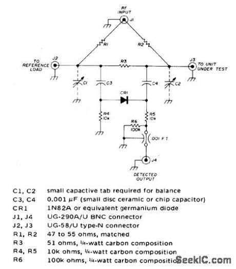
Works well through 450 MHz to for measuring and matching VHF and UHF antennas. If identical load impedances are placed at J2 and J3, signals at opposite ends of R3 are equal and in phase and there is no output at J4. If impedances are different, output proportional to difference appears at J4 Impedance values can be from 25 to 100 ohms, although drcuit is designed for optimum performance at 50 ohms.-J. Reisert, Matching Techniques for VHF/UHF Antennas, Ham Radio, July 1976, p 50-56. (View)
View full Circuit Diagram | Comments | Reading(1179)
FIELD_STRENGTH_AT_7_MHz
Published:2009/6/28 22:04:00 Author:May

Operates from single dry cell, Meter can be calibrated in decibels with Hewlett-Packard 606A or equivalent signal generator,Jack permits remote metering L1 is 5 turns、and L2 is 30 turns wound onAmidonT68-2 core.-R,W Jones、A7-MHz Vertical Parasitic Array QST,Nov,1973、p 39-43and 52 (View)
View full Circuit Diagram | Comments | Reading(761)
VARIABLE_ZENER_DIODE
Published:2009/6/28 22:01:00 Author:May
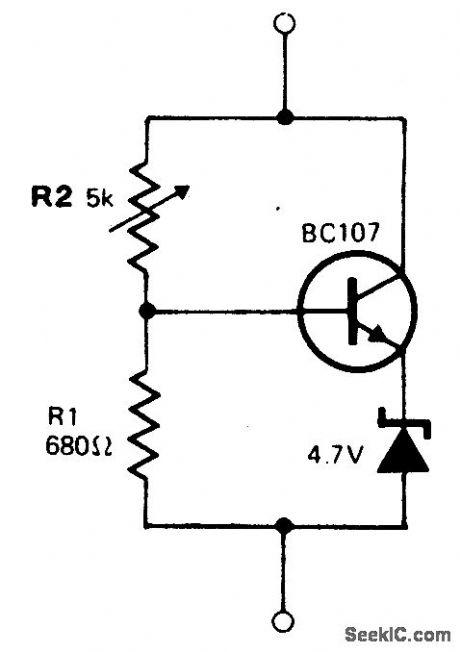
The circuit behaves like a zener diode over a large range of voltages. The current passing through the voltage divider R1-R2 is substantially larger than the transistor base current and is in the region of 8 mA. The stabilizing voltage is adjustable over the range 5-45 V by changing the value of R2. The total current drawn by the circuit is variable over the range 15 mA to 50 mA. This value is determined by the maximum dissipation of the zener diode. In the case of a 250 mW device, this is of the order of 50 mA. (View)
View full Circuit Diagram | Comments | Reading(201)
50_V/60_A_25_kHz_SWITCHING_REGULATOR_WITH_SEPARATE_ULTRA_STABLE_REFERENCE
Published:2009/6/28 21:31:00 Author:May
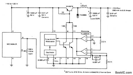
View full Circuit Diagram | Comments | Reading(809)
BAR_DISPLAY_WITH_ALARM_FLASHER
Published:2009/6/28 21:21:00 Author:May
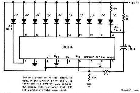
View full Circuit Diagram | Comments | Reading(986)
SINGLE_ENDED_REGULATOR
Published:2009/6/28 21:20:00 Author:May
In this conventional single-ended regulator circuit,the two outputs of the SG1524 are connected in parallel for effective 0-90%duty-cycle modulation. The use of an output inductor requlres an RC phase compensation network for loop stability. (View)
View full Circuit Diagram | Comments | Reading(896)
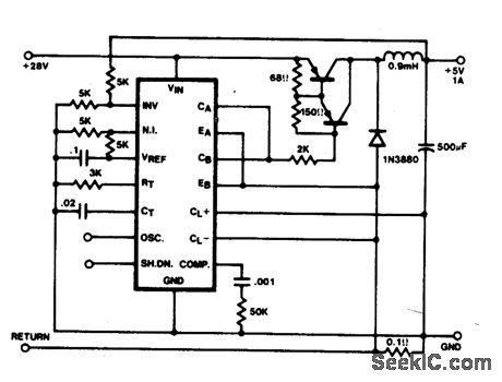
SWITCHING_STEP_DOWN_REGULATOR
Published:2009/6/28 21:18:00 Author:May
View full Circuit Diagram | Comments | Reading(752)
SPEED_TRAP
Published:2009/6/28 21:17:00 Author:May
Time required for auto to activate sensors placed measured distance apart on driveway or road is used to energize relay or alarm circuit when auto exceeds predetermined speed. If speed limit chosen is 15 mph, set detectors 22 feet apart for travel time of 1 s. Sensors can be photocells or air-actuated solenoids. For most applications, R1 can be 1-megohm pot. Transistor type is not critical. Values of R2 and C2 determine how long alarm sounds.-J. Sandier, 9 Projects under $9, Modem Electronics, Sept. 1978, p 35-39. (View)
View full Circuit Diagram | Comments | Reading(1696)
DIP_METER_USING_SILICON_JUNCTION_FET
Published:2009/6/28 21:13:00 Author:May
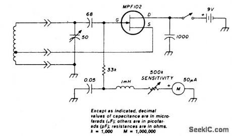
View full Circuit Diagram | Comments | Reading(1014)
SOLID_STATE_AUTO_REGULATOR
Published:2009/6/28 21:06:00 Author:May
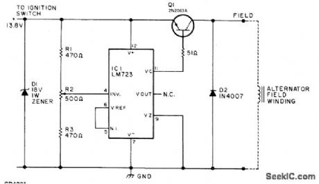
Replaces and outperforms electromechanical charging-voltage regulator in autos using altemator systems. Prolongs battery life by preventing un dercharging or overcharging of 12-V lead-acid battery. Uses LM723 connected as sia;itching regulatorfor controlling altematorfield cument. R2 is adjusted to maintain 13.8.V fully charged voltage for standard auto battery. Article gives construction details and tells how to use external relay to maintain altemator charge-indica-torfunction in cars having idiot light ratherthan charge-discharge ammeter. Q1 is 2N2063A (SK3009) 10-A PNP transistor.-W. J. Prudhomme, Build Your Own Car Regulator, 73 Magazine, March 1977, p 160-162. (View)
View full Circuit Diagram | Comments | Reading(0)
REMOTE_FLASH_TRIGGER
Published:2009/6/28 21:01:00 Author:May

Transistor Q1 is a light-activated silicon-controlled rectifier (LASCR). The gate is tripped by light entering a small lens built into the top cap. To operate, provide a 6-in. length of stiff wire for the anode and cathode connections and terminate the wires in a polarized power plug that matches the sync terminals on your electronic flashgun (strobelight). Make certain the anode lead connects to the positive sync terminal. When using the device, bend the connecting wires so the LASCR lens faces the main flash. This will fire the remote unit. (View)
View full Circuit Diagram | Comments | Reading(0)
0°TO_360°PHASE_SHIFTER
Published:2009/6/28 20:45:00 Author:May
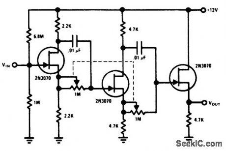
Each stage provides 0°to 180°phase shift. By ganging the two stages,0°to 360°phase shift is achieved.The 2N3070 JFETs do not load the phase shift networks. (View)
View full Circuit Diagram | Comments | Reading(894)
PHASE_SHIFT_CIRCUITS
Published:2009/6/28 20:43:00 Author:May
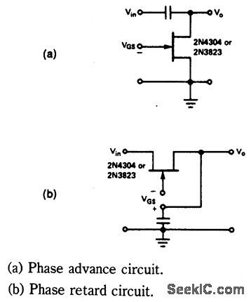
View full Circuit Diagram | Comments | Reading(834)
PRECISION_PHASE_SPLITTER
Published:2009/6/28 20:42:00 Author:May
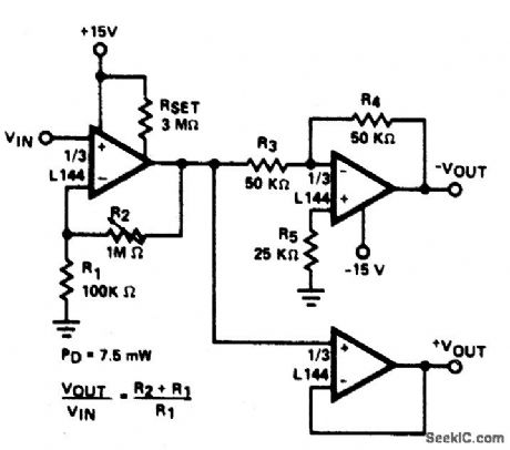
View full Circuit Diagram | Comments | Reading(1)
| Pages:6/24 1234567891011121314151617181920Under 20 |
Circuit Categories
power supply circuit
Amplifier Circuit
Basic Circuit
LED and Light Circuit
Sensor Circuit
Signal Processing
Electrical Equipment Circuit
Control Circuit
Remote Control Circuit
A/D-D/A Converter Circuit
Audio Circuit
Measuring and Test Circuit
Communication Circuit
Computer-Related Circuit
555 Circuit
Automotive Circuit
Repairing Circuit