
Analog Circuit
Index 7
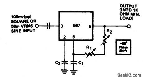
0°TO_180°PHASE_SHIFTER
Published:2009/6/28 20:42:00 Author:May
View full Circuit Diagram | Comments | Reading(754)
8_V_FROM_5_V_REGULATOR
Published:2009/6/26 5:05:00 Author:May
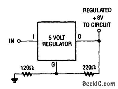
If you have trouble locating an 8-V regulator, although they are commonly available, a 5-V unit can replace it by connecting the regulator, as is shown here. (View)
View full Circuit Diagram | Comments | Reading(0)
SYNCHRONOUS_STEPDOWN_SWITCHING_REGULATOR_WITH_90%EFFICIENCY
Published:2009/6/26 5:01:00 Author:May
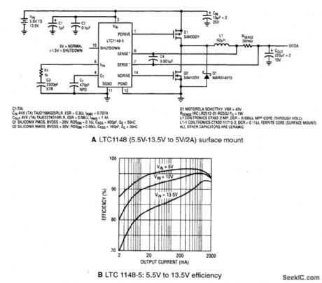
A shows a typical LTC1148 surface-mount application providing 5 V at 2 A from an input voltage of 5.5 V to 13.5 V. The operating efficiency, shown in B, peaks at 97% and exceeds 90% from 10 mA to 2 A with a 10-V input. Q1 and Q2 comprise the main switch and synchronous switch, respectively, and inductor current is measured via the voltage drop across the current shunt. RSENSE is the key component used to set the output current capability according to the formuta IOUT = 100 mV/RSENSE. The advantages of current control include excellent line and load transient rejection, inherent shortcircuit protection and controlled startup currents. Peak inductor current is limited to 150 mV/RSENSE or 3 A for the circuit in A. (View)
View full Circuit Diagram | Comments | Reading(695)
REGULATOR_LOSS_CUTTER
Published:2009/6/26 4:55:00 Author:May
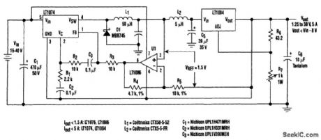
Large input-to-output voltage differentials, caused by wide input voltage variations, reduce a linear regulator's efficiency and increase its power dissipation. A switching preregulator can reduce this power dissipation by minimizing the voltage drop across an adjustable linear regulator to a constant 1.5-V value.
The circuit operates the LT1084 at slightly above its dropout voltage. To rninimize power dissipation, a low-dropout linear reg-ulator was chosen. The LT1084 functions as a conventional adjustable linear regulator with an output voltage that can be varied from 1.25 to 30 V.
Without the preregulator (for a 40-V input and a 5-V output at 5 A), it would be virtually impossible to find a heatsink large enough to dissipate enough energy to keep the linear-regulator junction temperature below its maximum value. With the prereg-ulator technique, however, the linear regulator will dissipate only 7.5 W under worst-case loading conditions for the entire input-voltage range of 15 to 40 V. Even under a short-circuit fault condition, the 1.5-V drop across the LT1084 is maintained. (View)
View full Circuit Diagram | Comments | Reading(2311)
DIODELESS_RECTIFIER
Published:2009/6/26 4:39:00 Author:May
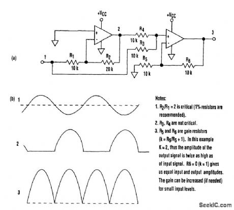
It's common knowledge that when working with single-supply op amps, implementing simple functions in a bipolar signal environment can be difficult. Sometimes additional op amps and other electronic components are required.
Taking that into consideration, can any advantage be attained from this mode? The answer lies in this simple circuit (A). Requiring no diodes, the circuit is a high-precision full-wave rectifier with a high-frequency limitation equalling that of the op amps themselves. Look at the circuit's timing diagram (B) to see the principle of operation.
The first amplifier rectifies negative input Ievels with an inverting gain of 2 and tums positive levels to zero. The second amp, a noninverting surnrning amplifier, adds the inverted negative signal from the first amplifier to the original input signal. The net result is the traditional waveform produced by full-wave rectification.
In spite of the lirnitation on the input signal amplitude (it must be less than VCC/2), this circuit can be useful in a variety of setups. (View)
View full Circuit Diagram | Comments | Reading(1338)
SHORTWAVE_FET_BOOSTER
Published:2009/6/26 4:26:00 Author:May
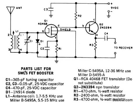
This two transistor preselector provides up to 40 dB gain from 3.5 to 30 MHz. Q1 (MOSFET) is sensitive to static charges and must be handled with care. (View)
View full Circuit Diagram | Comments | Reading(1176)
LOW_PARTS_COUNT_RATIOMETRIC_RESISTANCE_MEASUREMENT
Published:2009/6/26 4:04:00 Author:May
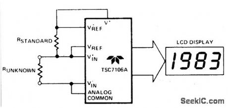
The unknown resistance is put in series with a known standard and a current passed through the pair. The voltage developed across the unknown is applied to the input and the voltage across the known resistor applied to the reference input. If the unknown equals the standard, the display will read 1000. The dis-played reading can be determined from the following expression:Runknown
Displayed Reading= ___________ =×1000 RstandardThe display will overrange for Runknown, ≥2× Rstandard. (View)
View full Circuit Diagram | Comments | Reading(0)
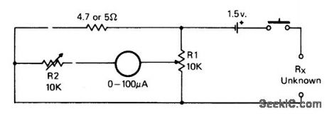
OHMMETER
Published:2009/6/26 4:00:00 Author:May
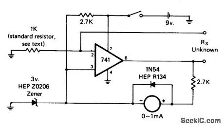
This circuit has a linear reading scale, requires no calibration, and requires no zero adjustment. It may be made multirange by switching in different standard resistors. (View)
View full Circuit Diagram | Comments | Reading(3122)
02μW_TO_10_mW
Published:2009/6/26 4:00:00 Author:May
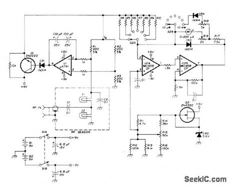
Accurate low-power wattmeter uses small lamps as barretters for measuring RF power up to 10mW from 1 to 500MHz. Applications indude measurements of antenna gain, local oscillator frequency, VSWR, and filter response. Subminiature T-3/4 RF sensor lamps operate in bridge circuit with R1, B2, and R3. Voltage difference between bridge legs is amplified by opamp U1. Bridge current driver Q1 supplies current for balancing bridge. Equilibrium voltage of 3.5 V at VB is fed to metering circuit including U2. Article covers calculation of values for calibration resistors R4-R10, which range from 5.715 to 7192 ohms.-J. H. Bowen, Accurate Low Power RF Wattmeter for High Fre-quency and VHF Measurements, Ham Radio, Dec. 1977, p 38-43. (View)
View full Circuit Diagram | Comments | Reading(862)
ANTENNA_ROTATOR_1
Published:2009/6/26 3:59:00 Author:May
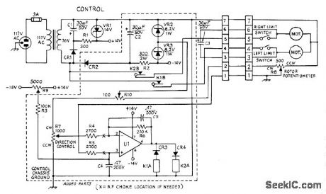
Developed for use with CDE TR-44 antenna control using low-voltage AC motor having pot for bearing indication. Circuit eliminates need for holding control handle in position until antenna reaches desired bearing. Uses 12-VDC 1000-ohm 1-A relays, TISN7274IL opamp U1, and wirewound 360° rotation command pot R7 operating from 14-V regulated supply of original control. When R7 is set to desired new heading, relay applies power to motor for proper direction, and drops out when antenna reaches desired heading. One relay is used for each direction of rotation.Opamp is connected in differential-input mode that responds only to difference voltage between wipers of pots R7 and R8. Polarity of oparnpoutput dependson polarity of input voltage difference. CR3 and CR4 energize K1 or K2 depending on polarity of error signal. R9 and R3 serve to balance voltage difference remaining when R7 and fi8 are at travel limits. R9 also nulls offset present when there is no input to U1. Ac-curacy is about 5°. Diodes are 100-PIV 0.5-A silicon.-K. H. Sucker, Automating the TR-44 An-tenna Rotor, QST, June 1973, p 28-30. (View)
View full Circuit Diagram | Comments | Reading(2544)
LINEAR_SCALE_OHMMETER_1
Published:2009/6/26 3:59:00 Author:May
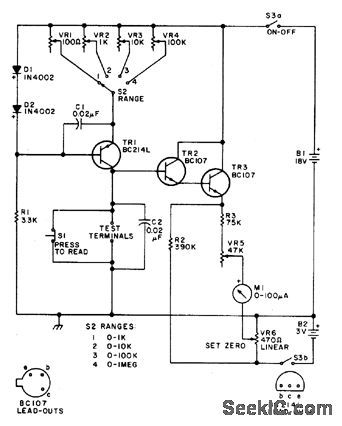
This circuit is designed to provide accu-rate measurement and a linear resistance scale at the high end. The circuit has four ranges.Another meter with a current range of 10 μA to 10 mA and sensitivity of 10,000 ohms per volt is needed for setting up. (View)
View full Circuit Diagram | Comments | Reading(0)
VOLTAGE_DOUBLER_SUPPLY
Published:2009/6/26 3:56:00 Author:May
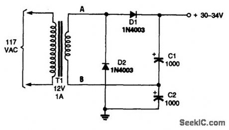
The voltage doubler is built around a pair of diodes (D1 and D2) and a pair of capacitors (C1 and C2) that are fed from, in this case, a 12-V, 1-A step-down transformer (T1). (View)
View full Circuit Diagram | Comments | Reading(770)
BRIDGE_CIRCUIT
Published:2009/6/26 3:55:00 Author:May
For measurement of resistances from about 5 ohms down to about 1/10 ohm. (View)
View full Circuit Diagram | Comments | Reading(0)
VLF_CONVERTER
Published:2009/6/26 3:51:00 Author:May
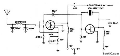
This converter uses a low-pass filter instead of the usual tuned circuit so the only tuning required is with the receiver. The dual-gate MOSFET and FET used in the mixer and oscillator aren't critical. Any crystal having a frequency compatible with the receiver tuning range may be used. For example, with a 3500 kHz crystal, 3500 kHz on the receiver dial corresponds to zero kHz; 3600 to 100 kHz; 3700 to 200 kHz, etc. (At 3500 khz on the receiver all one can hear is the converter os-cillator, and VLF signals start to come in about 20 kHz higher.) (View)
View full Circuit Diagram | Comments | Reading(0)
CURRENT_LIMITING_REGULATOR
Published:2009/6/26 3:49:00 Author:May
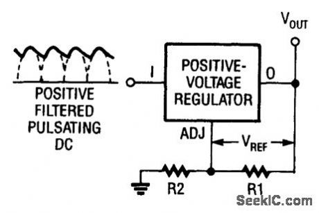
Floating adjustable regulators can be used as current Iimiters. Resistor R1 programs the current flowing through R2. (View)
View full Circuit Diagram | Comments | Reading(0)
ANALOG_RECEIVER_LOW_TEMPERATURE_DRIFT
Published:2009/6/26 3:41:00 Author:May
View full Circuit Diagram | Comments | Reading(0)
DIP_MEITR_USING
Published:2009/6/26 3:04:00 Author:May
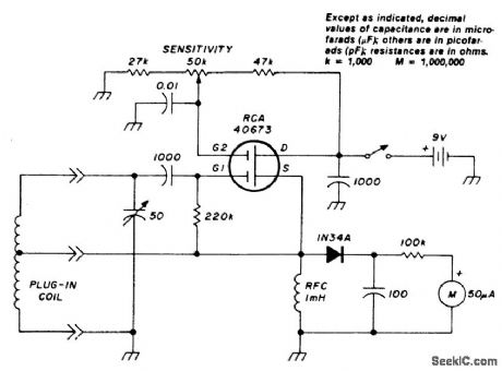
Circuit NotesGate 2 is used to adjust the oscillation level. (View)
View full Circuit Diagram | Comments | Reading(809)
NOISE_BRIDGE
Published:2009/6/26 2:31:00 Author:May


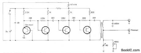
Used with communication receiver to measure impedance at antenna terminals or at end of transmission line, as required for adjusting antenna matching and loading devices for desired impedance at specific frequency. Consists of diode.connected transistor broadband,noise generator, 3-stage noise amplifier, and toroid transformer bridge.
All transistors are 2N5129 or equivalent 2N5137 or 2N5220. Try different transistors until highest noise output is obtained. Toroid core for trans.former is 3/8-inch Indiana General CF102. Quadrifilar winding has 4 1/2 turns of four No.28 enamel wires twisted together, wound on core and connected as on diagram. Noise bridge can also serve as wideband noise source for signal injection during troubleshooting in AF or RF circults, and as noise source for aligning RF cir-cuits,-J.J. Schultz, An Improved Antenna Noise Bridge, CQ, Sept, 1976, p 27-29 and 75. (View)
View full Circuit Diagram | Comments | Reading(0)
CAPACITIVE_ANTENNA
Published:2009/6/26 2:31:00 Author:May
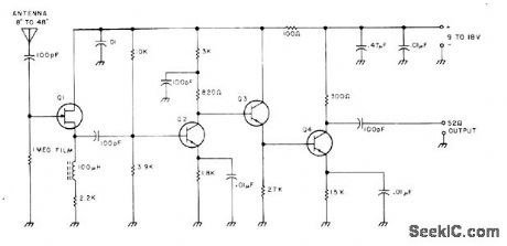
Cornbination of short whip antenna and broadband amplifier gives antenna covering entire range of 3 to 30 MHz without frequency selectivity. at is 2N3819 FET source follower driving three-transistor amplifier using 2N918, 2N6008, or other 200-MHz 20V NPN transistors to provide 30-dB gain. Circuit rolloff starts at 3 and 35 MHz. High gain of am plifier makes combination simulate quarter-wave whip over entire frequency range.-R. C.Wilson, The Incredible 18 All-Band Antenna, 73 Magazine, March 1975, p 49-50. (View)
View full Circuit Diagram | Comments | Reading(3151)
DRAWING_CIRCLES_ON_ASCOPE
Published:2009/6/26 2:23:00 Author:May
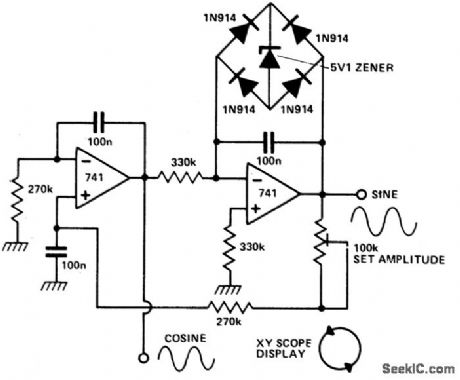
The circuit is that of a quadrature sine and cosine oscillator. To generate circular displays, connect the two outputs to the X and Y inputs. (View)
View full Circuit Diagram | Comments | Reading(887)
| Pages:7/24 1234567891011121314151617181920Under 20 |
Circuit Categories
power supply circuit
Amplifier Circuit
Basic Circuit
LED and Light Circuit
Sensor Circuit
Signal Processing
Electrical Equipment Circuit
Control Circuit
Remote Control Circuit
A/D-D/A Converter Circuit
Audio Circuit
Measuring and Test Circuit
Communication Circuit
Computer-Related Circuit
555 Circuit
Automotive Circuit
Repairing Circuit